SLOS070D July 1979 – November 2014 NE5534 , NE5534A , SA5534 , SA5534A
PRODUCTION DATA.
- 1 Features
- 2 Applications
- 3 Description
- 4 Simplified Schematic
- 5 Revision History
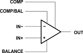
- 6 Pin Configuration and Functions
- 7 Specifications
- 8 Detailed Description
- 9 Application and Implementation
- 10Power Supply Recommendations
- 11Layout
- 12Device and Documentation Support
- 13Mechanical, Packaging, and Orderable Information
Package Options
Refer to the PDF data sheet for device specific package drawings
Mechanical Data (Package|Pins)
- D|8
- P|8
Thermal pad, mechanical data (Package|Pins)
Orderable Information
1 Features
- Equivalent Input Noise Voltage
3.5 nV/√Hz Typ - Unity-Gain Bandwidth 10 MHz Typ
- Common-Mode Rejection Ratio 100 dB Typ
- High DC Voltage Gain 100 V/mV Typ
- Peak-to-Peak Output Voltage Swing 32 V Typ With VCC± = ±18 V and RL = 600 Ω
- High Slew Rate 13 V/μs Typ
- Wide Supply-Voltage Range ±3 V to ±20 V
- Low Harmonic Distortion
- Offset Nulling Capability
- External Compensation Capability
2 Applications
- Audio Preamplifiers
- Servo Error Amplifiers
- Medical Equipment
- Telephone Channel Amplifiers
3 Description
The NE5534, NE5534A, SA5534, and SA5534A devices are high-performance operational amplifiers combining excellent dc and ac characteristics. Some of the features include very low noise, high output-drive capability, high unity-gain and maximum-output-swing bandwidths, low distortion, and high slew rate.
These operational amplifiers are compensated internally for a gain equal to or greater than three. Optimization of the frequency response for various applications can be obtained by use of an external compensation capacitor between COMP and COMP/BAL. The devices feature input-protection diodes, output short-circuit protection, and offset-voltage nulling capability with use of the BALANCE and COMP/BAL pins (see Figure 10).
For the NE5534A and SA5534A devices, a maximum limit is specified for the equivalent input noise voltage.
Device Information
| PART NUMBER | PACKAGE (PIN) | BODY SIZE (NOM) |
|---|---|---|
| NE5534x | SOIC (8) | 4.90 mm × 3.91 mm |
| SA5534x | SOIC (8) | 4.90 mm × 3.91 mm |
| SO (8) | 6.20 mm × 5.30 mm |
4 Simplified Schematic