SLOS795F September 2013 – October 2017 TAS5414C-Q1
PRODUCTION DATA.
- 1 Features
- 2 Applications
- 3 Description
- 4 Revision History
- 5 Pin Configuration and Functions
- 6 Specifications
- 7 Detailed Description
- 8 Application and Implementation
- 9 Power Supply Recommendations
- 10Layout
- 11Device and Documentation Support
- 12Mechanical, Packaging, and Orderable Information
Package Options
Refer to the PDF data sheet for device specific package drawings
Mechanical Data (Package|Pins)
- PHD|64
Thermal pad, mechanical data (Package|Pins)
- PHD|64
Orderable Information
6 Specifications
6.1 Absolute Maximum Ratings
over operating free-air temperature range (unless otherwise noted)| VALUE | UNIT | ||||
|---|---|---|---|---|---|
| MIN | MAX | ||||
| PVDD | DC supply voltage range | Relative to GND | –0.3 | 30 | V |
| PVDDMAX | Pulsed supply voltage range | t ≤ 100 ms exposure | –1 | 50 | V |
| PVDDRAMP | Supply voltage ramp rate | 15 | V/ms | ||
| IPVDD | Externally imposed dc supply current per PVDD or GND pin | ±12 | A | ||
| IPVDD_MAX | Pulsed supply current per PVDD pin (one shot) | t < 100 ms | 17 | A | |
| IO | Maximum allowed dc current per output pin | ±13.5 | A | ||
| IO_MAX (1) | Pulsed output current per output pin (single pulse) | t < 100 ms | ±17 | A | |
| IIN_MAX | Maximum current, all digital and analog input pins(2) | DC or pulsed | ±1 | mA | |
| IMUTE_MAX | Maximum current on MUTE pin | DC or pulsed | ±20 | mA | |
| IIN_ODMAX | Maximum sink current for open-drain pins | 7 | mA | ||
| VLOGIC | Input voltage range for pin relative to GND (SCL, SDA, I2C_ADDR pins) | Supply voltage range: 6V < PVDD < 24 V |
–0.3 | 6 | V |
| VMUTE | Voltage range for MUTE pin relative to GND | Supply voltage range: 6 V < PVDD < 24 V |
–0.3 | 7.5 | V |
| VSTANDBY | Input voltage range for STANDBY pin | Supply voltage range: 6 V < PVDD < 24 V |
–0.3 | 5.5 | V |
| VOSC_SYNC | Input voltage range for OSC_SYNC pin relative to GND | Supply voltage range: 6 V < PVDD < 24 V |
–0.3 | 3.6 | V |
| VGND | Maximum voltage between GND pins | ±0.3 | V | ||
| VAIN_AC_MAX_5414 | Maximum ac-coupled input voltage for TAS5414C-Q1(2), analog input pins | Supply voltage range: 6 V < PVDD < 24 V |
1.9 | Vrms | |
| VAIN_AC_MAX_5424 | Maximum ac-coupled differential input voltage for TAS5424C-Q1(2), analog input pins | Supply voltage range: 6 V < PVDD < 24 V |
3.8 | Vrms | |
| TJ | Maximum operating junction temperature range | –55 | 150 | °C | |
| Tstg | Storage temperature | –55 | 150 | °C | |
(1) Pulsed current ratings are maximum survivable currents externally applied to the device. The device may encounter high currents during reverse-battery, fortuitous open-ground, and fortuitous open-supply fault conditions.
(2) See the Application Information section for information on analog input voltage and ac coupling.
6.2 ESD Ratings
| VALUE | UNIT | ||||
|---|---|---|---|---|---|
| V(ESD) | Electrostatic discharge | Human body model (HBM), per AEC Q100-002(1) | ±2500 | V | |
| Charged device model (CDM), per AEC Q100-011 DKE Package |
Corner pins excluding OSC_SYNC | ±1000 | V | ||
| All other pins (including OSC_SYNC) except CP pin | ±500 | ||||
| CP pin (Non-Corner Pin) | ±400 | ||||
| Charged device model (CDM), per AEC Q100-011 PHD Package |
Corner pins excluding SCL | ±750 | V | ||
| All pins (including SCL) except CP and CP_Top | ±600 | ||||
| CP and CP_Top pins | ±400 | ||||
(1) AEC Q100-002 indicates HBM stressing is done in accordance with the ANSI/ESDA/JEDEC JS-001 specification.
6.3 Recommended Operating Conditions(1)
| MIN | TYP | MAX | UNIT | |||
|---|---|---|---|---|---|---|
| PVDDOP | DC supply voltage range relative to GND | 6 | 14.4 | 24 | V | |
| VAIN_5414 (2) | Analog audio input signal level (TAS5414C-Q1) | AC-coupled input voltage | 0 | 0.25–1(3) | Vrms | |
| VAIN_5424 (2) | Analog audio input signal level (TAS5424C-Q1) | AC-coupled input voltage | 0 | 0.5–2(3) | Vrms | |
| TA | Ambient temperature | –40 | 105 | °C | ||
| TJ | Junction temperature | An adequate heat sink is required to keep TJ within specified range. | –40 | 115 | °C | |
| RL | Nominal speaker load impedance | 2 | 4 | Ω | ||
| VPU | Pullup voltage supply (for open-drain logic outputs) | 3 | 3.3 or 5 | 5.5 | V | |
| RPU_EXT | External pullup resistor on open-drain logic outputs | Resistor connected between open-drain logic output and VPU supply | 10 | 50 | kΩ | |
| RPU_I2C | I2C pullup resistance on SDA and SCL pins | 1 | 4.7 | 10 | kΩ | |
| RI2C_ADD | Total resistance of voltage divider for I2C address slave 1 or slave 2, connected between D_BYP and GND pins | 10 | 50 | kΩ | ||
| RREXT | External resistance on REXT pin | 1% tolerance required | 19.8 | 20 | 20.2 | kΩ |
| CD_BYP , CA_BYP |
External capacitance on D_BYP and A_BYP pins | 10 | 120 | nF | ||
| COUT | External capacitance to GND on OUT_X pins | 150 | 680 | nF | ||
| CIN | External capacitance to analog input pin in series with input signal | 0.47 | μF | |||
| CFLY | Flying capacitor on charge pump | 0.47 | 1 | 1.5 | μF | |
| CP | Charge pump capacitor | 50V needed for Load Dump | 0.47 | 1 | 1.5 | μF |
| CMUTE | MUTE pin capacitor | 100 | 220 | 1000 | nF | |
| COSCSYNC_MAX | Allowed loading capacitance on OSC_SYNC pin | 75 | pF | |||
(1) The Recommended Operating Conditions table specifies only that the device is functional in the given range. See the Electrical Characteristics table for specified performance limits.
(2) Signal input for full unclipped output with gains of 32 dB, 26 dB, 20 dB, and 12 dB
(3) Maximum recommended input voltage is determined by the gain setting.
6.4 Thermal Information
| PARAMETER | VALUE (Typical) | UNIT | |
|---|---|---|---|
| RθJC | Junction-to-case (heat slug) thermal resistance, DKE package | 1 | °C/W |
| RθJC | Junction-to-case (heat slug) thermal resistance, PHD package | 1.2 | |
| RθJA | Junction-to-ambient thermal resistance | This device is not intended to be used without a heatsink. Therefore, RθJA is not specified. Refer to the Thermal Information section. | |
| Exposed pad dimensions, DKE package | 13.8 × 5.8 | mm | |
| Exposed pad dimensions, PHD package | 8 × 8 | ||
6.5 Electrical Characteristics
Test conditions (unless otherwise noted): TCase = 25°C, PVDD = 14.4 V, RL = 4 Ω, fS = 417 kHz, Pout = 1 W/ch, Rext = 20 kΩ, AES17 filter, default I2C settings, master-mode operation (see Figure 21)| PARAMETER | TEST CONDITIONS | MIN | TYP | MAX | UNIT | |
|---|---|---|---|---|---|---|
| OPERATING CURRENT | ||||||
| IPVDD_IDLE | PVDD idle current | All four channels in MUTE mode | 170 | 220 | mA | |
| IPVDD_Hi-Z | All four channels in Hi-Z mode | 93 | ||||
| IPVDD_STBY | PVDD standby current | STANDBY mode, TJ ≤ 85°C | 2 | 10 | μA | |
| OUTPUT POWER | ||||||
| POUT | Output power per channel | 4 Ω, PVDD = 14.4 V, THD+N ≤ 1%, 1 kHz, Tc = 75°C | 23 | W | ||
| 4 Ω, PVDD = 14.4 V, THD+N = 10%, 1 kHz, Tc = 75°C | 25 | 28 | ||||
| 4 Ω, PVDD = 24 V, THD+N = 10%, 1 kHz, Tc = 75°C | 63 | 79 | ||||
| 2 Ω, PVDD = 14.4 V, THD+N = 1%, 1 kHz, Tc = 75°C | 38 | |||||
| 2 Ω, PVDD = 14.4 V, THD+N = 10%, 1 kHz, Tc = 75°C | 40 | 50 | ||||
| PBTL 2-Ω operation, PVDD = 24 V, THD+N = 10%, 1 kHz, Tc = 75°C | 150 | |||||
| PBTL 1-Ω operation, PVDD = 14.4 V, THD+N = 10%, 1 kHz, Tc = 75°C | 90 | |||||
| EFFP | Power efficiency | 4 channels operating, 23-W output power/ch, L = 10 μH, TJ ≤ 85°C | 90% | |||
| AUDIO PERFORMANCE | ||||||
| VNOISE | Noise voltage at output | Zero input, and A-weighting | 60 | 100 | μV | |
| Channel crosstalk | P = 1 W, f = 1 kHz, enhanced crosstalk enabled via I2C (reg. 0x10) | 70 | 85 | dB | ||
| CMRR5424 | Common-mode rejection ratio (TAS5424C-Q1) | f = 1 kHz, 1 Vrms referenced to GND, G = 26 dB | 60 | 75 | dB | |
| PSRR | Power-supply rejection ratio | PVDD = 14.4 Vdc + 1 Vrms, f = 1 kHz | 60 | 75 | dB | |
| THD+N | Total harmonic distortion + noise | P = 1 W, f = 1 kHz | 0.02% | 0.1% | ||
| fS | Switching frequency | Switching frequency selectable for AM interference avoidance | 336 | 357 | 378 | kHz |
| 392 | 417 | 442 | ||||
| 470 | 500 | 530 | ||||
| RAIN | Analog input resistance | Internal shunt resistance on each input pin | 63 | 85 | 106 | kΩ |
| VIN_CM | Common-mode input voltage | AC-coupled common-mode input voltage (zero differential input) | 1.3 | Vrms | ||
| VCM_INT | Internal common-mode input bias voltage | Internal bias applied to IN_M pin | 3.3 | V | ||
| G | Voltage gain (VO/VIN) | Source impedance = 0 Ω, gain measurement taken at 1 W of power per channel | 11 | 12 | 13 | dB |
| 19 | 20 | 21 | ||||
| 25 | 26 | 27 | ||||
| 31 | 32 | 33 | ||||
| GCH | Channel-to-channel variation | Any gain commanded | –1 | 0 | 1 | dB |
| PWM OUTPUT STAGE | ||||||
| RDS(on) | FET drain-to-source resistance | Not including bond wire resistance, TJ = 25°C | 65 | 90 | mΩ | |
| VO_OFFSET | Output offset voltage | Zero input signal, G = 26 dB | ±10 | ±50 | mV | |
| PVDD OVERVOLTAGE (OV) PROTECTION | ||||||
| VOV_SET | PVDD overvoltage shutdown set | 24.6 | 26.4 | 28.2 | V | |
| VOV_CLEAR | PVDD overvoltage shutdown clear | 24.4 | 25.9 | 27.4 | V | |
| PVDD UNDERVOLTAGE (UV) PROTECTION | ||||||
| VUV_SET | PVDD undervoltage shutdown set | 4.9 | 5.3 | 5.6 | V | |
| VUV_CLEAR | PVDD undervoltage shutdown clear | 6.2 | 6.6 | 7 | V | |
| AVDD | ||||||
| VA_BYP | A_BYP pin voltage | 6.5 | V | |||
| VA_BYP_UV_SET | A_BYP UV voltage | 4.8 | V | |||
| VA_BYP_UV_CLEAR | Recovery voltage A_BYP UV | 5.3 | V | |||
| DVDD | ||||||
| VD_BYP | D_BYP pin voltage | 3.3 | V | |||
| POWER-ON RESET (POR) | ||||||
| VPOR | PVDD voltage for POR | I2C active above this voltage | 4 | V | ||
| VPOR_HY | PVDD recovery hysteresis voltage for POR | 0.1 | V | |||
| REXT | ||||||
| VREXT | Rext pin voltage | 1.27 | V | |||
| CHARGE PUMP (CP) | ||||||
| VCPUV_SET | CP undervoltage | 4.8 | V | |||
| VCPUV_CLEAR | Recovery voltage for CP UV | 4.9 | V | |||
| OVERTEMPERATURE (OT) PROTECTION | ||||||
| TOTW1_CLEAR | Junction temperature for overtemperature warning | 96 | 112 | 128 | °C | |
| TOTW1_SET / TOTW2_CLEAR |
106 | 122 | 138 | °C | ||
| TOTW2_SET / TOTW3_CLEAR |
116 | 132 | 148 | °C | ||
| TOTW3_SET / TOTSD_CLEAR |
126 | 142 | 158 | °C | ||
| TOTSD | Junction temperature for overtemperature shutdown | 136 | 152 | 168 | °C | |
| TFB | Junction temperature for overtemperature foldback | Per channel | 130 | 150 | 170 | °C |
| CURRENT LIMITING PROTECTION | ||||||
| ILIM | Current limit (load current) | Level 1 | 5.5 | 7.3 | 9 | A |
| Level 2 (default) | 10.6 | 12.7 | 15 | |||
| OVERCURRENT (OC) SHUTDOWN PROTECTION | ||||||
| IMAX | Maximum current (peak output current) | Level 1 | 7.8 | 9.8 | 12.2 | A |
| Level 2 (default), Any short to supply, ground, or other channels | 11.9 | 14.8 | 17.7 | |||
| TWEETER DETECT | ||||||
| ITH_TW | Load-current threshold for tweeter detect | 330 | 445 | 560 | mA | |
| ILIM_TW | Load-current limit for tweeter detect | 2.1 | A | |||
| STANDBY MODE | ||||||
| VIH | STANDBY input voltage for logic-level high | 2 | V | |||
| VIL | STANDBY input voltage for logic-level low | 0.7 | V | |||
| ISTBY | STANDBY pin current | 0.1 | 0.2 | μA | ||
| MUTE MODE | ||||||
| GMUTE | Output attenuation | MUTE pin ≤ 0.5 V for 200ms or I2C Mute Enabled | 100 | dB | ||
| DC DETECT | ||||||
| VTH_DC_TOL | DC detect threshold tolerance | 25% | ||||
| tDCD | DC detect step-response time for four channels | 5.3 | s | |||
| CLIP_OTW REPORT | ||||||
| VOH_CLIPOTW | CLIP_OTW pin output voltage for logic level high (open-drain logic output) | External 47-kΩ pullup resistor to 3 V–5.5 V | 2.4 | V | ||
| VOL_CLIPOTW | CLIP_OTW pin output voltage for logic level low (open-drain logic output) | 0.5 | V | |||
| tDELAY_CLIPDET | CLIP_OTW signal delay when output clipping detected | 20 | μs | |||
| FAULT REPORT | ||||||
| VOH_FAULT | FAULT pin output voltage for logic-level high (open-drain logic output) | External 47-kΩ pullup resistor to 3 V–5.5 V | 2.4 | V | ||
| VOL_FAULT | FAULT pin output voltage for logic-level low (open-drain logic output) | 0.5 | ||||
| OPEN, SHORT DIAGNOSTICS | ||||||
| RS2P, RS2G | Maximum resistance to detect a short from OUT pin(s) to PVDD or ground | 200 | Ω | |||
| ROPEN_LOAD | Minimum load resistance to detect open circuit | Including speaker wires | 300 | 740 | 1300 | Ω |
| RSHORTED_LOAD | Maximum load resistance to detect short circuit | Including speaker wires | 0.5 | 1 | 1.5 | Ω |
| I2C ADDRESS DECODER | ||||||
| tLATCH_I2CADDR | Time delay to latch I2C address after POR | 300 | μs | |||
| VI2C_ADDR | Voltage on I2C_ADDR pin for address 0 | Connect to GND | 0% | 0% | 15% | VD_BYP |
| Voltage on I2C_ADDR pin for address 1 | External resistors in series between D_BYP and GND as a voltage divider | 25% | 35% | 45% | ||
| Voltage on I2C_ADDR pin for address 2 | 55% | 65% | 75% | |||
| Voltage on I2C_ADDR pin for address 3 | Connect to D_BYP | 85% | 100% | 100% | ||
| I2C | ||||||
| tHOLD_I2C | Power-on hold time before I2C communication | STANDBY high | 1 | ms | ||
| fSCL | SCL clock frequency | 400 | kHz | |||
| VIH | SCL pin input voltage for logic-level high | RPU_I2C = 5-kΩ pullup, supply voltage = 3.3 V or 5 V | 2.1 | 5.5 | V | |
| VIL | SCL pin input voltage for logic-level low | –0.5 | 1.1 | V | ||
| VOH | SDA pin output voltage for logic-level high | I2C read, RI2C = 5-kΩ pullup, supply voltage = 3.3 V or 5 V |
2.4 | V | ||
| VO | SDA pin output voltage for logic-level low | I2C read, 3-mA sink current | 0.4 | V | ||
| VIH | SDA pin input voltage for logic-level high | I2C write, RI2C = 5-kΩ pullup, supply voltage = 3.3 V or 5 V |
2.1 | 5.5 | V | |
| VIL | SDA pin input voltage for logic-level low | I2C write, RI2C = 5-kΩ pullup, supply voltage = 3.3 V or 5 V |
–0.5 | 1.1 | V | |
| C I | Capacitance for SCL and SDA pins | 10 | pF | |||
| OSCILLATOR | ||||||
| VOH | OSC_SYNC pin output voltage for logic-level high | I2C_ADDR pin set to MASTER mode | 2.4 | V | ||
| VOL | OSC_SYNC pin output voltage for logic-level low | 0.5 | V | |||
| VIH | OSC_SYNC pin input voltage for logic-level high | I2C_ADDR pin set to SLAVE mode | 2 | V | ||
| VIL | OSC_SYNC pin input voltage for logic-level low | 0.8 | V | |||
| fOSC_SYNC | OSC_SYNC pin clock frequency | I2C_ADDR pin set to MASTER mode, fS = 500 kHz | 3.76 | 4 | 4.24 | MHz |
| I2C_ADDR pin set to MASTER mode, fS = 417 kHz | 3.13 | 3.33 | 3.63 | |||
| I2C_ADDR pin set to MASTER mode, fS = 357 kHz | 2.68 | 2.85 | 3.0 | |||
6.6 Timing Requirements for I2C Interface Signals
over recommended operating conditions (unless otherwise noted)| MIN | TYP | MAX | UNIT | ||
|---|---|---|---|---|---|
| tr | Rise time for both SDA and SCL signals | 300 | ns | ||
| tf | Fall time for both SDA and SCL signals | 300 | ns | ||
| tw(H) | SCL pulse duration, high | 0.6 | μs | ||
| tw(L) | SCL pulse duration, low | 1.3 | μs. | ||
| tsu2 | Setup time for START condition | 0.6 | μs | ||
| th2 | START condition hold time until generation of first clock pulse | 0.6 | μs | ||
| tsu1 | Data setup time | 100 | ns | ||
| th1 | Data hold time | 0(1) | ns | ||
| tsu3 | Setup time for STOP condition | 0.6 | μs | ||
| CB | Load capacitance for each bus line | 400 | pF | ||
(1) A device must internally provide a hold time of at least 300 ns for the SDA signal to bridge the undefined region of the falling edge of SCL.
 Figure 1. SCL and SDA Timing
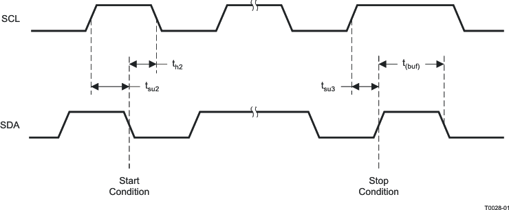 Figure 2. Timing for Start and Stop Conditions
6.7 Typical Characteristics
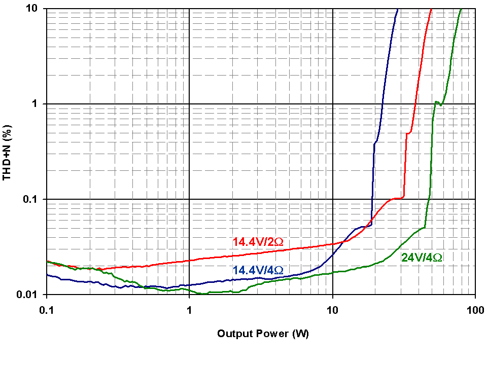 Figure 3. THD+N vs BTL Output Power at 1kHz
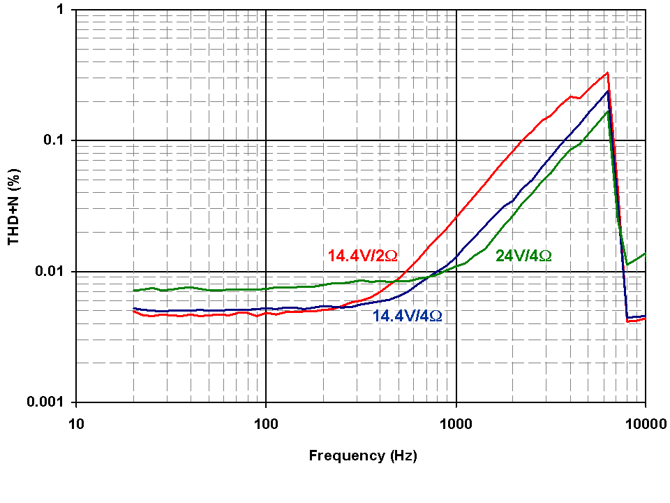 Figure 5. THD+N vs Frequency at 1 Watt
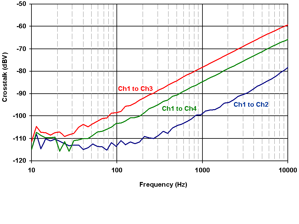 Figure 7. Crosstalk vs Frequency
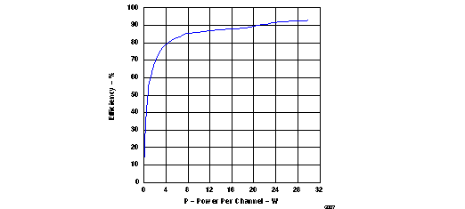 Figure 9. Efficiency
Four Channels AT 4 Ω Each
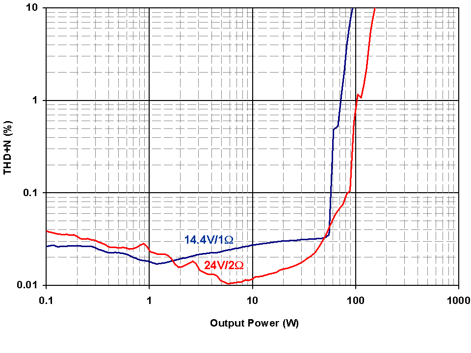 Figure 4. THD+N vs PBTL Output Power at 1kHz
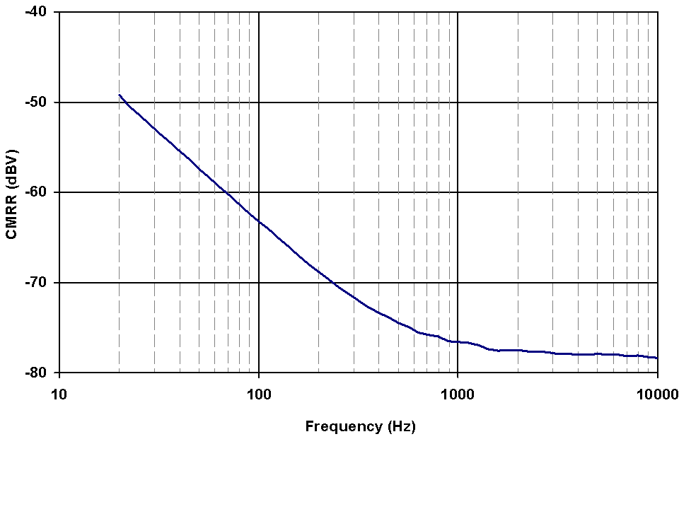 Figure 6. TAS5424C-Q1
Common-Mode Rejection Ratio vs Frequency
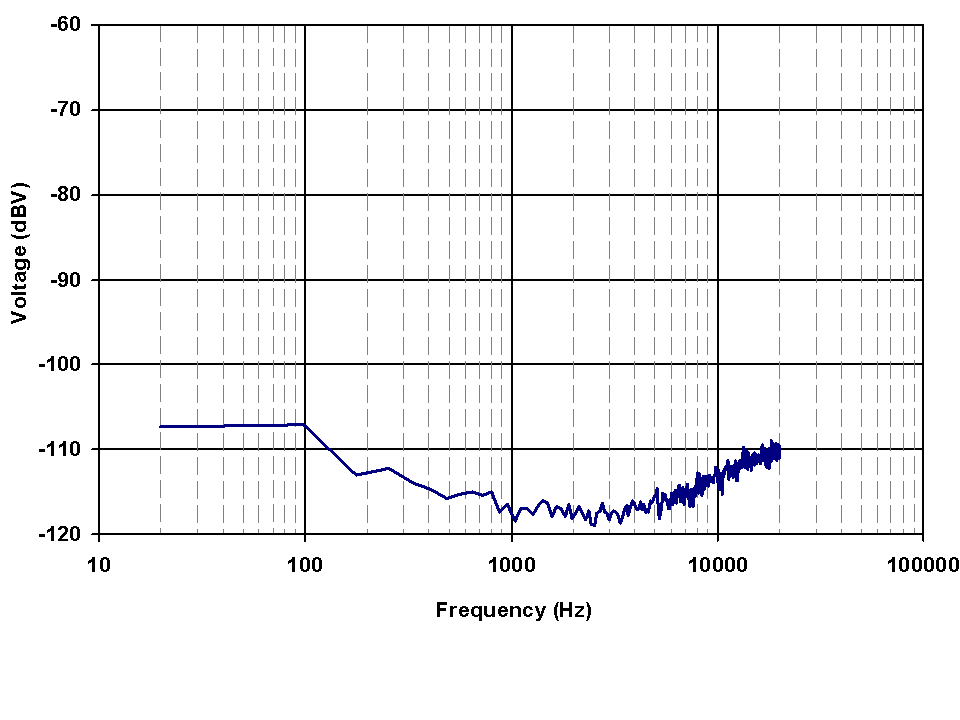 Figure 8. Noise FFT
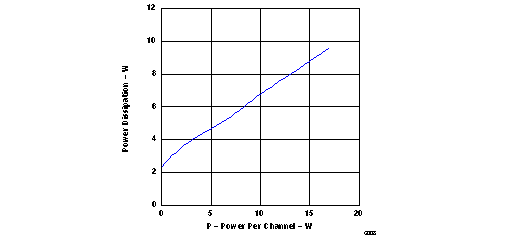 Figure 10. Device Power Dissipation
Four Channels at 4 Ω Each