Find TI packages
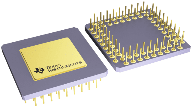
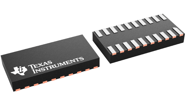
TI’s broad packaging portfolio supports thousands of diversified products, packaging configurations and technologies. These packages include traditional ceramic and leaded options and advanced chip scale packages (Quad Flat No Lead (QFN), Wafer Chip Scale Package (WCSP) or Die-Size Ball Grid Array (DSBGA)), using fine pitch wire bond and flip chip interconnects, with SiP, module, stacked and embedded die formats.
Select a package family below to view the options, or search all TI packages to explore TI’s complete package portfolio. A complete description of TI package families can be found here. A selection of the industry's smallest devices, based on our small package technologies, is also available below.
Small form factor for low-to-moderate pin count devices
Flat, square body with leads or pads on all four size and no exposed pad
Designing a compact signal chain for high performance in small spaces
Engineers are often challenged with making system designs smaller or packing additional functionality in the same amount of printed circuit board (PCB) space. This white paper addresses the key design considerations for working with small-package analog products to help you understand how you can leverage the benefits of these smaller devices in your design.


