SCES888C May   2018  – May 2024 2N7001T

PRODUCTION DATA  

  1.   1
  2. Features
  3. Applications
  4. Description
  5. Pin Configuration and Functions
  6. Specifications
    1. 5.1 Absolute Maximum Ratings
    2. 5.2 ESD Ratings
    3. 5.3 Recommended Operating Conditions
    4. 5.4 Thermal Information
    5. 5.5 Electrical Characteristics
    6. 5.6 Switching Characteristics
    7. 5.7 Operating Characteristics
    8. 5.8 Typical Characteristics
  7. Parameter Measurement Information
    1. 6.1 Load Circuit and Voltage Waveforms
  8. Detailed Description
    1. 7.1 Overview
    2. 7.2 Functional Block Diagram
    3. 7.3 Feature Description
      1. 7.3.1 Up-Translation or Down-Translation from 1.65 V to 3.60 V
      2. 7.3.2 Balanced CMOS Push-Pull Outputs
      3. 7.3.3 Standard CMOS Inputs
      4. 7.3.4 Negative Clamping Diodes
      5. 7.3.5 Partial Power Down (Ioff)
      6. 7.3.6 Over-voltage Tolerant Inputs
    4. 7.4 Device Functional Modes
  9. Application and Implementation
    1. 8.1 Application Information
    2. 8.2 Typical Applications
      1. 8.2.1 Processor Error Up Translation
        1. 8.2.1.1 Design Requirements
        2. 8.2.1.2 Detailed Design Procedure
        3. 8.2.1.3 Application Curve
      2. 8.2.2 Discrete FET Translation Replacement
    3. 8.3 Power Supply Recommendations
    4. 8.4 Layout
      1. 8.4.1 Layout Guidelines
      2. 8.4.2 Layout Example
  10. Device and Documentation Support
    1. 9.1 Documentation Support
      1. 9.1.1 Related Documentation
    2. 9.2 Receiving Notification of Documentation Updates
    3. 9.3 Support Resources
    4. 9.4 Trademarks
    5. 9.5 Electrostatic Discharge Caution
    6. 9.6 Glossary
  11. 10Revision History
  12. 11Mechanical, Packaging, and Orderable Information

Package Options

Mechanical Data (Package|Pins)
Thermal pad, mechanical data (Package|Pins)
Orderable Information

Negative Clamping Diodes

The inputs and outputs to this device have negative clamping diodes as shown in Figure 7-1.

CAUTION:

Voltages beyond the values specified in the Absolute Maximum Ratings table can cause damage to the device. The input negative-voltage and output voltage ratings may be exceeded if the input and output clamp-current ratings are observed.
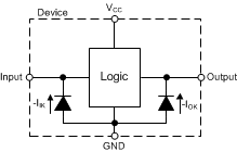
2N7001T Electrical Placement of Clamping Diodes for Each Input and OutputFigure 7-1 Electrical Placement of Clamping Diodes for Each Input and Output