SNAS825A December 2021 – April 2022 ADC128S102-SEP
PRODUCTION DATA
- 1 Features
- 2 Applications
- 3 Description
- 4 Revision History
- 5 Pin Configuration and Functions
- 6 Specifications
- 7 Detailed Description
- 8 Application and Implementation
- 9 Power Supply Recommendations
- 10Layout
- 11Device and Documentation Support
- 12Mechanical, Packaging, and Orderable Information
Package Options
Mechanical Data (Package|Pins)
- PW|16
Thermal pad, mechanical data (Package|Pins)
Orderable Information
7.4.1 ADC128S102-SEP Operation
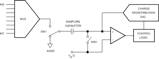
Simplified schematics of the ADC128S102-SEP in both track and hold operation are provided in Figure 7-3 and Figure 7-4, respectively. In Figure 7-3, the ADC128S102-SEP is in track mode: switch SW1 connects the sampling capacitor to one of eight analog input channels through the multiplexer, and SW2 balances the comparator inputs. The ADC128S102-SEP is in this state for the first three SCLK cycles after CS is brought low.
 Figure 7-3 ADC128S102-SEP in Track
Mode
Figure 7-3 ADC128S102-SEP in Track
ModeFigure 7-4 shows the ADC128S102-SEP in hold mode: switch SW1 connects the sampling capacitor to ground, maintaining the sampled voltage, and switch SW2 unbalances the comparator. The control logic then instructs the charge-redistribution DAC to add or subtract fixed amounts of charge to or from the sampling capacitor until the comparator is balanced. When the comparator is balanced, the digital word supplied to the DAC is the digital representation of the analog input voltage. The ADC128S102-SEP is in this state for the last 13 SCLK cycles after CS is brought low.
 Figure 7-4 ADC128S102-SEP in Hold Mode