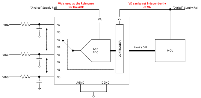
The ADC128S102 is a low-power, eight-channel CMOS 12-bit analog-to-digital converter specified for conversion throughput rates of 500 ksps to 1 MSPS. The converter is based on a successive-approximation register architecture with an internal track-and-hold circuit. It can be configured to accept up to eight input signals at inputs IN0 through IN7.
The output serial data is straight binary and is compatible with several standards, such as SPI, QSPI, MICROWIRE, and many common DSP serial interfaces.
The ADC128S102 may be operated with independent analog and digital supplies. The analog supply (VA) can range from +2.7 V to +5.25 V, and the digital supply (VD) can range from +2.7 V to VA. Normal power consumption using a +3-V or +5-V supply is 2.3 mW and 10.7 mW, respectively. The power-down feature reduces the power consumption to 0.06 µW using a +3-V supply and 0.25 µW using a +5-V supply.
The ADC128S102 is packaged in a 16-lead TSSOP package. Operation over the extended industrial temperature range of −40°C to +105°C is ensured.
PART NUMBER | PACKAGE | BODY SIZE (NOM) |
---|---|---|
ADC128S102 | TSSOP (16) | 5.00 mm x 4.40 mm |
Changes from F Revision (May 2013) to G Revision
Changes from D Revision (March 2013) to E Revision
PIN | I/O | DESCRIPTION | |
---|---|---|---|
NO. | NAME | ||
3 | AGND | Supply | The ground return for the analog supply and signals. |
1 | CS | IN | Chip select. On the falling edge of CS, a conversion process begins. Conversions continue as long as CS is held low. |
12 | DGND | Supply | The ground return for the digital supply and signals. |
14 | DIN | IN | Digital data input. The ADC128S102's Control Register is loaded through this pin on rising edges of the SCLK pin. |
15 | DOUT | OUT | Digital data output. The output samples are clocked out of this pin on the falling edges of the SCLK pin. |
4 - 11 | IN0 to IN7 | IN | Analog inputs. These signals can range from 0 V to VREF. |
16 | SCLK | IN | Digital clock input. The ensured performance range of frequencies for this input is 8 MHz to 16 MHz. This clock directly controls the conversion and readout processes. |
2 | VA | Supply | Positive analog supply pin. This voltage is also used as the reference voltage. This pin should be connected to a quiet +2.7-V to +5.25-V source and bypassed to GND with 1-µF and 0.1-µF monolithic ceramic capacitors located within 1 cm of the power pin. |
13 | VD | Supply | Positive digital supply pin. This pin should be connected to a +2.7 V to VA supply, and bypassed to GND with a 0.1-µF monolithic ceramic capacitor located within 1 cm of the power pin. |
MIN | MAX | UNIT | ||
---|---|---|---|---|
Analog Supply Voltage VA | −0.3 | 6.5 | V | |
Digital Supply Voltage VD | −0.3 | VA + 0.3, max 6.5 | V | |
Voltage on Any Pin to GND | −0.3 | VA +0.3 | V | |
Input Current at Any Pin (3) | –10 | 10 | mA | |
Package Input Current(3) | –20 | 20 | mA | |
Power Dissipation at TA = 25°C | See (4) | |||
Junction Temperature | 150 | °C | ||
Storage temperature, Tstg | −65 | 150 | °C | |
For soldering specifications: see product folder at www.ti.com and SNOA549 |
VALUE | UNIT | |||
---|---|---|---|---|
V(ESD) | Electrostatic discharge | Human body model (HBM), per ANSI/ESDA/JEDEC JS-001(1) | ±2500 | V |
Machine model (MM) | ±250 |
MIN | MAX | UNIT | |
---|---|---|---|
Operating Temperature, TA | –40 | 105 | °C |
VA Supply Voltage | 2.7 | 5.25 | V |
VD Supply Voltage | 2.7 | VA | V |
Digital Input Voltage | 0 | VA | V |
Analog Input Voltage | 0 | VA | V |
Clock Frequency | 8 | 16 | MHz |
THERMAL METRIC(1) | ADC128S102 | UNIT | |
---|---|---|---|
PW | |||
16 PINS | |||
RθJA | Junction-to-ambient thermal resistance | 110 | °C/W |
RθJC(top) | Junction-to-case (top) thermal resistance | 42 | |
RθJB | Junction-to-board thermal resistance | 56 | |
ψJT | Junction-to-top characterization parameter | 5 | |
ψJB | Junction-to-board characterization parameter | 55 |
PARAMETER | TEST CONDITIONS | MIN | TYP | MAX(1) | UNIT | |
---|---|---|---|---|---|---|
STATIC CONVERTER CHARACTERISTICS | ||||||
Resolution with No Missing Codes | 12 | Bits | ||||
INL | Integral Non-Linearity (End Point Method) | VA = VD = +3.0V | –1 | ±0.4 | 1 | LSB |
VA = VD = +5.0V | –1.2 | ±0.5 | 1.2 | LSB | ||
DNL | Differential Non-Linearity | VA = VD = +3.0V | +0.4 | 0.9 | LSB | |
−0.7 | −0.2 | LSB | ||||
VA = VD = +5.0V | +0.7 | 1.5 | LSB | |||
−0.9 | −0.4 | LSB | ||||
VOFF | Offset Error | VA = VD = +3.0V | –2.3 | +0.8 | 2.3 | LSB |
VA = VD = +5.0V | –2.3 | +1.1 | 2.3 | LSB | ||
OEM | Offset Error Match | VA = VD = +3.0V | –1.5 | ±0.1 | 1.5 | LSB |
VA = VD = +5.0V | –1.5 | ±0.3 | 1.5 | LSB | ||
FSE | Full Scale Error | VA = VD = +3.0V | –2.0 | +0.8 | 2.0 | LSB |
VA = VD = +5.0V | –2.0 | +0.3 | 2.0 | LSB | ||
FSEM | Full Scale Error Match | VA = VD = +3.0V | –1.5 | ±0.1 | 1.5 | LSB |
VA = VD = +5.0V | –1.5 | ±0.3 | 1.5 | LSB | ||
DYNAMIC CONVERTER CHARACTERISTICS | ||||||
FPBW | Full Power Bandwidth (−3dB) | VA = VD = +3.0V | 8 | MHz | ||
VA = VD = +5.0V | 11 | MHz | ||||
SINAD | Signal-to-Noise Plus Distortion Ratio | VA = VD = +3.0V, fIN = 40.2 kHz, −0.02 dBFS |
70 | 73 | dB | |
VA = VD = +5.0V, fIN = 40.2 kHz, −0.02 dBFS |
70 | 73 | dB | |||
SNR | Signal-to-Noise Ratio | VA = VD = +3.0V, fIN = 40.2 kHz, −0.02 dBFS |
70.8 | 73 | dB | |
VA = VD = +5.0V, fIN = 40.2 kHz, −0.02 dBFS |
70.8 | 73 | dB | |||
THD | Total Harmonic Distortion | VA = VD = +3.0V, fIN = 40.2 kHz, −0.02 dBFS |
−88 | −74 | dB | |
VA = VD = +5.0V, fIN = 40.2 kHz, −0.02 dBFS |
−90 | −74 | dB | |||
SFDR | Spurious-Free Dynamic Range | VA = VD = +3.0V, fIN = 40.2 kHz, −0.02 dBFS |
75 | 91 | dB | |
VA = VD = +5.0V, fIN = 40.2 kHz, −0.02 dBFS |
75 | 92 | dB | |||
ENOB | Effective Number of Bits | VA = VD = +3.0V, fIN = 40.2 kHz |
11.3 | 11.8 | Bits | |
VA = VD = +5.0V, fIN = 40.2 kHz, −0.02 dBFS |
11.3 | 11.8 | Bits | |||
ISO | Channel-to-Channel Isolation | VA = VD = +3.0V, fIN = 20 kHz |
82 | dB | ||
VA = VD = +5.0V, fIN = 20 kHz, −0.02 dBFS |
84 | dB | ||||
IMD | Intermodulation Distortion, Second Order Terms | VA = VD = +3.0V, fa = 19.5 kHz, fb = 20.5 kHz |
−89 | dB | ||
VA = VD = +5.0V, fa = 19.5 kHz, fb = 20.5 kHz |
−91 | dB | ||||
Intermodulation Distortion, Third Order Terms | VA = VD = +3.0V, fa = 19.5 kHz, fb = 20.5 kHz |
−88 | dB | |||
VA = VD = +5.0V, fa = 19.5 kHz, fb = 20.5 kHz |
−88 | dB | ||||
ANALOG INPUT CHARACTERISTICS | ||||||
VIN | Input Range | 0 to VA | V | |||
IDCL | DC Leakage Current | –1 | 1 | µA | ||
CINA | Input Capacitance | Track Mode | 33 | pF | ||
Hold Mode | 3 | pF | ||||
DIGITAL INPUT CHARACTERISTICS | ||||||
VIH | Input High Voltage | VA = VD = +2.7V to +3.6V | 2.1 | V | ||
VA = VD = +4.75V to +5.25V | 2.4 | V | ||||
VIL | Input Low Voltage | VA = VD = +2.7V to +5.25V | 0.8 | V | ||
IIN | Input Current | VIN = 0V or VD | –1 | ±0.01 | 1 | µA |
CIND | Digital Input Capacitance | 2 | 4 | pF | ||
DIGITAL OUTPUT CHARACTERISTICS | ||||||
VOH | Output High Voltage | ISOURCE = 200 µA, VA = VD = +2.7V to +5.25V |
VD − 0.5 | V | ||
VOL | Output Low Voltage | ISINK = 200 µA to 1.0 mA, VA = VD = +2.7V to +5.25V |
0.4 | V | ||
IOZH, IOZL | Hi-Impedance Output Leakage Current | VA = VD = +2.7V to +5.25V | –1 | 1 | µA | |
COUT | Hi-Impedance Output Capacitance (2) | 2 | 4 | pF | ||
Output Coding | Straight (Natural) Binary | |||||
POWER SUPPLY CHARACTERISTICS (CL = 10 pF) | ||||||
VA, VD | Analog and Digital Supply Voltages | VA ≥ VD | 2.7 | 5.25 | V | |
IA + ID | Total Supply Current Normal Mode ( CS low) |
VA = VD = +2.7V to +3.6V, fSAMPLE = 1 MSPS, fIN = 40 kHz |
0.76 | 1.5 | mA | |
VA = VD = +4.75V to +5.25V, fSAMPLE = 1 MSPS, fIN = 40 kHz |
2.13 | 3.1 | mA | |||
Total Supply Current Shutdown Mode (CS high) |
VA = VD = +2.7V to +3.6V, fSCLK = 0 ksps |
20 | nA | |||
VA = VD = +4.75V to +5.25V, fSCLK = 0 ksps |
50 | nA | ||||
PC | Power Consumption Normal Mode ( CS low) |
VA = VD = +3.0V fSAMPLE = 1 MSPS, fIN = 40 kHz |
2.3 | 4.5 | mW | |
VA = VD = +5.0V fSAMPLE = 1 MSPS, fIN = 40 kHz |
10.7 | 15.5 | mW | |||
Power Consumption Shutdown Mode (CS high) |
VA = VD = +3.0V fSCLK = 0 ksps |
0.06 | µW | |||
VA = VD = +5.0V fSCLK = 0 ksps |
0.25 | µW | ||||
AC ELECTRICAL CHARACTERISTICS | ||||||
fSCLKMIN | Minimum Clock Frequency | VA = VD = +2.7V to +5.25V | 8 | 0.8 | MHz | |
fSCLK | Maximum Clock Frequency | VA = VD = +2.7V to +5.25V | 16 | MHz | ||
fS | Sample Rate Continuous Mode |
VA = VD = +2.7V to +5.25V | 500 | 50 | ksps | |
1 | MSPS | |||||
tCONVERT | Conversion (Hold) Time | VA = VD = +2.7V to +5.25V | 13 | SCLK cycles | ||
DC | SCLK Duty Cycle | VA = VD = +2.7V to +5.25V | 40% | 30 | ||
70 | 60% | |||||
tACQ | Acquisition (Track) Time | VA = VD = +2.7V to +5.25V | 3 | SCLK cycles | ||
Throughput Time | Acquisition Time + Conversion Time VA = VD = +2.7V to +5.25V |
16 | SCLK cycles | |||
tAD | Aperture Delay | VA = VD = +2.7V to +5.25V | 4 | ns |
PARAMETER | TEST CONDITIONS | MIN | TYP | MAX(1) | UNIT | |
---|---|---|---|---|---|---|
tCSH | CS Hold Time after SCLK Rising Edge | 10 | 0 | ns | ||
tCSS | CS Setup Time prior to SCLK Rising Edge | 10 | 4.5 | ns | ||
tEN | CS Falling Edge to DOUT enabled | 5 | 30 | ns | ||
tDACC | DOUT Access Time after SCLK Falling Edge | 17 | 27 | ns | ||
tDHLD | DOUT Hold Time after SCLK Falling Edge | 4 | ns | |||
tDS | DIN Setup Time prior to SCLK Rising Edge | 10 | 3 | ns | ||
tDH | DIN Hold Time after SCLK Rising Edge | 10 | 3 | ns | ||
tCH | SCLK High Time | 0.4 x tSCLK | ns | |||
tCL | SCLK Low Time | 0.4 x tSCLK | ns | |||
tDIS | CS Rising Edge to DOUT High-Impedance | DOUT falling | 2.4 | 20 | ns | |
DOUT rising | 0.9 | 20 | ns |
The ADC128S102 is a successive-approximation analog-to-digital converter designed around a charge-redistribution digital-to-analog converter.
Simplified schematics of the ADC128S102 in both track and hold operation are shown in Figure 34 and Figure 35 respectively. In Figure 34, the ADC128S102 is in track mode: switch SW1 connects the sampling capacitor to one of eight analog input channels through the multiplexer, and SW2 balances the comparator inputs. The ADC128S102 is in this state for the first three SCLK cycles after CS is brought low.
Figure 35 shows the ADC128S102 in hold mode: switch SW1 connects the sampling capacitor to ground, maintaining the sampled voltage, and switch SW2 unbalances the comparator. The control logic then instructs the charge-redistribution DAC to add or subtract fixed amounts of charge to or from the sampling capacitor until the comparator is balanced. When the comparator is balanced, the digital word supplied to the DAC is the digital representation of the analog input voltage. The ADC128S102 is in this state for the last thirteen SCLK cycles after CS is brought low.
The output format of the ADC128S102 is straight binary. Code transitions occur midway between successive integer LSB values. The LSB width for the ADC128S102 is VA / 4096. The ideal transfer characteristic is shown in Figure 36. The transition from an output code of 0000 0000 0000 to a code of 0000 0000 0001 is at 1/2 LSB, or a voltage of VA / 8192. Other code transitions occur at steps of one LSB.
An equivalent circuit for one of the ADC128S102's input channels is shown in Figure 37. Diodes D1 and D2 provide ESD protection for the analog inputs. The operating range for the analog inputs is 0 V to VA. Going beyond this range will cause the ESD diodes to conduct and result in erratic operation.
The capacitor C1 in Figure 37 has a typical value of 3 pF and is mainly the package pin capacitance. Resistor R1 is the on resistance of the multiplexer and track / hold switch and is typically 500 ohms. Capacitor C2 is the ADC128S102 sampling capacitor, and is typically 30 pF. The ADC128S102 will deliver best performance when driven by a low-impedance source (less than 100 ohms). This is especially important when using the ADC128S102 to sample dynamic signals. Also important when sampling dynamic signals is a band-pass or low-pass filter which reduces harmonics and noise in the input. These filters are often referred to as anti-aliasing filters.
The ADC128S102's digital inputs (SCLK, CS, and DIN) have an operating range of 0 V to VA. They are not prone to latch-up and may be asserted before the digital supply (VD) without any risk. The digital output (DOUT) operating range is controlled by VD. The output high voltage is VD - 0.5V (min) while the output low voltage is 0.4V (max).
The ADC128S102 is fully powered-up whenever CS is low and fully powered-down whenever CS is high, with one exception. If operating in continuous conversion mode, the ADC128S102 automatically enters power-down mode between SCLK's 16th falling edge of a conversion and SCLK's 1st falling edge of the subsequent conversion (see Figure 1).
In continuous conversion mode, the ADC128S102 can perform multiple conversions back to back. Each conversion requires 16 SCLK cycles and the ADC128S102 will perform conversions continuously as long as CS is held low. Continuous mode offers maximum throughput.
In burst mode, the user may trade off throughput for power consumption by performing fewer conversions per unit time. This means spending more time in power-down mode and less time in normal mode. By utilizing this technique, the user can achieve very low sample rates while still utilizing an SCLK frequency within the electrical specifications. The Power Consumption vs. SCLK curve in the Typical Characteristics section shows the typical power consumption of the ADC128S102. To calculate the power consumption (PC), simply multiply the fraction of time spent in the normal mode (tN) by the normal mode power consumption (PN), and add the fraction of time spent in shutdown mode (tS) multiplied by the shutdown mode power consumption (PS) as shown in Equation 1.
An operational timing diagram and a serial interface timing diagram for the ADC128S102 are shown in the Timing Specifications section. CS, chip select, initiates conversions and frames the serial data transfers. SCLK (serial clock) controls both the conversion process and the timing of serial data. DOUT is the serial data output pin, where a conversion result is sent as a serial data stream, MSB first. Data to be written to the ADC128S102's Control Register is placed on DIN, the serial data input pin. New data is written to DIN with each conversion.
A serial frame is initiated on the falling edge of CS and ends on the rising edge of CS. Each frame must contain an integer multiple of 16 rising SCLK edges. The ADC's DOUT pin is in a high impedance state when CS is high and is active when CS is low. Thus, CS acts as an output enable. Similarly, SCLK is internally gated off when CS is brought high.
During the first 3 cycles of SCLK, the ADC is in the track mode, acquiring the input voltage. For the next 13 SCLK cycles the conversion is accomplished and the data is clocked out. SCLK falling edges 1 through 4 clock out leading zeros while falling edges 5 through 16 clock out the conversion result, MSB first. If there is more than one conversion in a frame (continuous conversion mode), the ADC will re-enter the track mode on the falling edge of SCLK after the N*16th rising edge of SCLK and re-enter the hold/convert mode on the N*16+4th falling edge of SCLK. "N" is an integer value.
The ADC128S102 enters track mode under three different conditions. In Figure 1, CS goes low with SCLK high and the ADC enters track mode on the first falling edge of SCLK. In the second condition, CS goes low with SCLK low. Under this condition, the ADC automatically enters track mode and the falling edge of CS is seen as the first falling edge of SCLK. In the third condition, CS and SCLK go low simultaneously and the ADC enters track mode. While there is no timing restriction with respect to the rising edges of CS and SCLK, see Figure 3 for setup and hold time requirements for the falling edge of CS with respect to the rising edge of SCLK.
While a conversion is in progress, the address of the next input for conversion is clocked into a control register through the DIN pin on the first 8 rising edges of SCLK after the fall of CS. See Table 1, Table 2, and Table 3.
There is no need to incorporate a power-up delay or dummy conversions as the ADC128S102 is able to acquire the input signal to full resolution in the first conversion immediately following power-up. The first conversion result after power-up will be that of IN0.
Bit 7 (MSB) | Bit 6 | Bit 5 | Bit 4 | Bit 3 | Bit 2 | Bit 1 | Bit 0 |
---|---|---|---|---|---|---|---|
DONTC | DONTC | ADD2 | ADD1 | ADD0 | DONTC | DONTC | DONTC |
Bit No: | Symbol: | Description |
---|---|---|
7, 6, 2, 1, 0 | DONTC | Don't care. The values of these bits do not affect the device. |
5 | ADD2 | These three bits determine which input channel will be sampled and converted at the next conversion cycle. The mapping between codes and channels is shown in Table 3. |
4 | ADD1 | |
3 | ADD0 |
ADD2 | ADD1 | ADD0 | Input Channel |
---|---|---|---|
0 | 0 | 0 | IN0 (Default) |
0 | 0 | 1 | IN1 |
0 | 1 | 0 | IN2 |
0 | 1 | 1 | IN3 |
1 | 0 | 0 | IN4 |
1 | 0 | 1 | IN5 |
1 | 1 | 0 | IN6 |
1 | 1 | 1 | IN7 |