SNAS717A April 2017 – October 2021 ADC12D1620QML-SP
PRODUCTION DATA
- 1 Features
- 2 Applications
- 3 Description
- 4 Revision History
- 5 Pin Configuration and Functions
-
6 Specifications
- 6.1 Absolute Maximum Ratings
- 6.2 ESD Ratings
- 6.3 Recommended Operating Conditions
- 6.4 Thermal Information
- 6.5 Converter Electrical Characteristics: Static Converter Characteristics
- 6.6 Converter Electrical Characteristics: Dynamic Converter Characteristics
- 6.7 Converter Electrical Characteristics: Analog Input/Output and Reference Characteristics
- 6.8 Converter Electrical Characteristic: Channel-to-Channel Characteristics
- 6.9 Converter Electrical Characteristics: LVDS CLK Input Characteristics
- 6.10 Electrical Characteristics: AutoSync Feature
- 6.11 Converter Electrical Characteristics: Digital Control and Output Pin Characteristics
- 6.12 Converter Electrical Characteristics: Power Supply Characteristics
- 6.13 Converter Electrical Characteristics: AC Electrical Characteristics
- 6.14 Electrical Characteristics: Delta Parameters
- 6.15 Timing Requirements: Serial Port Interface
- 6.16 Timing Requirements: Calibration
- 6.17 Quality Conformance Inspection
- 6.18 Timing Diagrams
- 6.19 Typical Characteristics
-
7 Detailed Description
- 7.1 Overview
- 7.2 Functional Block Diagram
- 7.3 Feature Description
- 7.4 Device Functional Modes
- 7.5
Programming
- 7.5.1
Control Modes
- 7.5.1.1
Non-ECM
- 7.5.1.1.1 Dual-Edge Sampling Pin (DES)
- 7.5.1.1.2 Non-Demultiplexed Mode Pin (NDM)
- 7.5.1.1.3 Dual Data-Rate Phase Pin (DDRPh)
- 7.5.1.1.4 Calibration Pin (CAL)
- 7.5.1.1.5 Low-Sampling Power-Saving Mode Pin (LSPSM)
- 7.5.1.1.6 Power-Down I-Channel Pin (PDI)
- 7.5.1.1.7 Power-Down Q-Channel Pin (PDQ)
- 7.5.1.1.8 Test-Pattern Mode Pin (TPM)
- 7.5.1.1.9 Full-Scale Input-Range Pin (FSR)
- 7.5.1.1.10 AC- or DC-Coupled Mode Pin (VCMO)
- 7.5.1.1.11 LVDS Output Common-Mode Pin (VBG)
- 7.5.1.2 Extended Control Mode
- 7.5.1.1
Non-ECM
- 7.5.1
Control Modes
- 7.6 Register Maps
- 8 Application Information Disclaimer
- 9 Power Supply Recommendations
- 10Layout
- 11Device and Documentation Support
- 12Mechanical, Packaging, and Orderable Information
Package Options
Refer to the PDF data sheet for device specific package drawings
Mechanical Data (Package|Pins)
- FVA|256
- NAA|376
Thermal pad, mechanical data (Package|Pins)
Orderable Information
10.4 Board Mounting Recommendation
Proper thermal profile is required to establish re-flow under the package and ensure all joints meet profile specifications.
| RANGE UP | PEAK TEMPERATURE (TPK) | MAXIMUM PEAK TEMPERATURE | RAMP DOWN |
|---|---|---|---|
| ≤ 4°C/sec | 210°C ≤ tPK ≤ 215°C | ≤ 220°C | ≤ 5°C/sec |
The 220°C peak temperature is driven by the requirement to limit the dissolution of lead from the high-melt pin to the eutectic solder. Too much lead increases the effective melting point of the board-side joint and makes it much more difficult to remove the device if module rework is required.
Cool-down rates and methods affect CCGA assemble yield and reliability. Picking up boards or opening the oven while solder joints are in molten state can disturb the solder joint. Do not pick up boards until the solder joints have fully solidified. Board warping may potentially cause CCGA lifting off pads during cooling and this condition can also cause pin cracking when severe. This warping is a result of a high differential cooling rate between the top and bottom of the board. Both conditions can be prevented by using even top and bottom cooling.
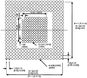
 Figure 10-5 Landing Pattern Recommendation