SLVSEO0C August 2021 – June 2024 ADC12DJ4000RF
PRODUCTION DATA
- 1
- 1 Features
- 2 Applications
- 3 Description
- 4 Device Comparison
- 5 Pin Configuration and Functions
-
6 Specifications
- 6.1 Absolute Maximum Ratings
- 6.2 ESD Ratings
- 6.3 Recommended Operating Conditions
- 6.4 Thermal Information
- 6.5 Electrical Characteristics: DC Specifications
- 6.6 Electrical Characteristics: Power Consumption
- 6.7 Electrical Characteristics: AC Specifications (Dual-Channel Mode)
- 6.8 Electrical Characteristics: AC Specifications (Single-Channel Mode)
- 6.9 Timing Requirements
- 6.10 Switching Characteristics
- 6.11 Typical Characteristics
-
7 Detailed Description
- 7.1 Overview
- 7.2 Functional Block Diagram
- 7.3
Feature Description
- 7.3.1 Analog Inputs
- 7.3.2 ADC Core
- 7.3.3 Temperature Monitoring Diode
- 7.3.4 Timestamp
- 7.3.5 Clocking
- 7.3.6 Programmable FIR Filter (PFIR)
- 7.3.7 Digital Down Converters (DDC)
- 7.3.8
JESD204C Interface
- 7.3.8.1 Transport Layer
- 7.3.8.2 Scrambler
- 7.3.8.3 Link Layer
- 7.3.8.4 8B/10B Link Layer
- 7.3.8.5
64B/66B Link Layer
- 7.3.8.5.1 64B/66B Encoding
- 7.3.8.5.2 Multiblocks, Extended Multiblocks and the Local Extended Multiblock Clock (LEMC)
- 7.3.8.5.3 Block, Multiblock and Extended Multiblock Alignment using Sync Header
- 7.3.8.5.4 Initial Lane Alignment
- 7.3.8.5.5 Block, Multiblock and Extended Multiblock Alignment Monitoring
- 7.3.8.6 Physical Layer
- 7.3.8.7 SerDes Pre-Emphasis
- 7.3.8.8 JESD204C Enable
- 7.3.8.9 Multi-Device Synchronization and Deterministic Latency
- 7.3.8.10 Operation in Subclass 0 Systems
- 7.3.9 Alarm Monitoring
- 7.4
Device Functional Modes
- 7.4.1 Dual-Channel Mode
- 7.4.2 Single-Channel Mode (DES Mode)
- 7.4.3 Dual-Input Single-Channel Mode (DUAL DES Mode)
- 7.4.4 JESD204C Modes
- 7.4.5 Power-Down Modes
- 7.4.6 Test Modes
- 7.4.7 Calibration Modes and Trimming
- 7.4.8 Offset Calibration
- 7.4.9 Trimming
- 7.5 Programming
- 7.6 SPI Register Map
- 8 Application Information Disclaimer
- 9 Device and Documentation Support
- 10Revision History
- 11Mechanical, Packaging, and Orderable Information
Package Options
Mechanical Data (Package|Pins)
- ZEG|144
- AAV|144
Thermal pad, mechanical data (Package|Pins)
Orderable Information
7.3.7.3 Decimation Filters
The decimation filters are arranged to provide a programmable overall decimation of 4 or 8. All decimation filters operate on complex data (from the complex digital mixer) and the outputs have a resolution of 15 bits. The decimation filters are implemented as linear phase finite impulse response (FIR) filters. Table 7-12 lists the effective output sample rates, available signal bandwidths, output formats, and stop-band attenuation for each decimation mode.
| DECIMATION SETTING | ƒ(DEVCLK) | OUTPUT FORMAT | |||
|---|---|---|---|---|---|
| OUTPUT RATE (MSPS) | MAX ALIAS PROTECTED SIGNAL BANDWIDTH (MHz) | STOP-BAND ATTENUATION | PASS-BAND RIPPLE | ||
| No decimation (DDC bypass) | ƒ(DEVCLK) | ƒ(DEVCLK) / 2 | — | < ±0.001 dB | Real signal, 12-bit data |
| Decimate-by-4 | ƒ(DEVCLK) / 4 | 0.8 × ƒ(DEVCLK) / 4 | > 90 dB | < ±0.001 dB | Complex signal, 15-bit data |
| Decimate-by-8 | ƒ(DEVCLK) / 8 | 0.8 × ƒ(DEVCLK) / 8 | > 90 dB | < ±0.001 dB | Complex signal, 15-bit data |
| Decimate-by-16 | ƒ(DEVCLK) / 16 | 0.8 × ƒ(DEVCLK) / 16 | > 90 dB | < ±0.001 dB | Complex signal, 15-bit data |
| Decimate-by-32 | ƒ(DEVCLK) / 32 | 0.8 × ƒ(DEVCLK) / 32 | > 90 dB | < ±0.001 dB | Complex signal, 15-bit data |
Figure 7-11 to Figure 7-18 provide the composite decimation filter responses. The black portion of the trace shows the pass-band region, or alias-protected region, of the response. The red portion of the trace shows the transition region of the response as well as any frequency regions that will alias into the transition region. The transition region is not alias protected and therefore desired signals should only be placed in the pass-band region of the filter response. The blue portion of the trace shows the frequency regions that will alias into the pass-band after decimation and therefore define the stop-band region of the frequency response. The stop-band attenuation is defined to sufficient filter any undesired images or signals to prevent them from aliasing into the desired pass-band. Use analog filtering before the analog inputs (INA± or INB±) for additional attenuation of signals that fall within this band or to sufficiently reduce signals at the ADC inputs that may produce harmonics, interleaving spurs or other undesired spurious signals that will alias into the desired signal band (before the complex mixing and decimation operations).
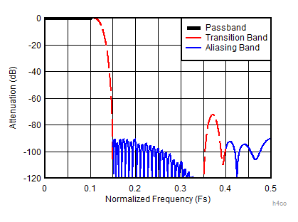 Figure 7-11 Decimate-by-4 Composite Response
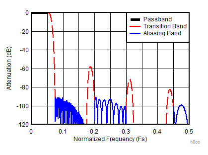 Figure 7-13 Decimate-by-8 Composite Response
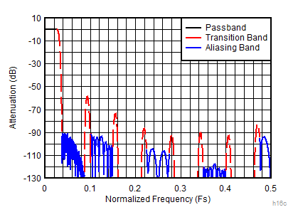 Figure 7-15 Decimate-by-16 Composite Response
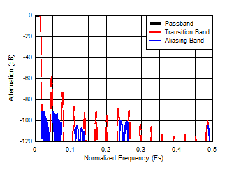 Figure 7-17 Decimate-by-32 Composite Response
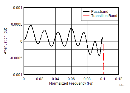 Figure 7-12 Decimate-by-4 Composite Zoomed Pass-Band Response
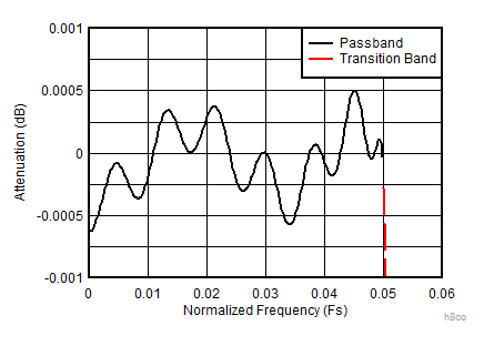 Figure 7-14 Decimate-by-8 Composite Zoomed Pass-Band Response
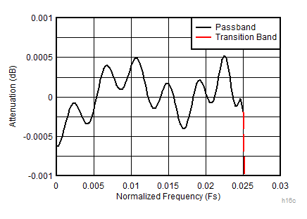 Figure 7-16 Decimate-by-16 Composite Zoomed Pass-Band Response
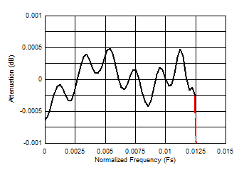 Figure 7-18 Decimate-by-32 Composite Zoomed Pass-Band Response
For maximum efficiency, a group of high-speed filter blocks are implemented with specific blocks used for each decimation setting to achieve the composite responses illustrated in Figure 7-11 to Figure 7-18. Table 7-13 describes the combination of filter blocks used for each decimation setting and Table 7-14 lists the coefficient details and decimation factor of each filter block. The coefficients are symmetric with the center tap indicated by bold text.
| DECIMATION SETTING | FILTER BLOCKS USED (Listed in Order of Operation) |
|---|---|
| 4 | CS40, CS80 |
| 8 | CS20, CS40, CS80 |
| 16 | CS10, CS20, CS40, CS80 |
| 32 | CS5, CS10, CS20, CS40, CS80 |
| FILTER COEFFICIENT SET (Decimation Factor of Filter, Scale factor) | |||||||||
|---|---|---|---|---|---|---|---|---|---|
| CS5 (2, 2-5) | CS10 (2, 2-11) | CS20 (2, 2-14) | CS40 (2, 2-17) | CS80 (2, 2-19) | |||||
| –1 | –1 | –65 | –65 | 109 | 109 | –327 | –327 | –37 | –37 |
| 0 | 0 | 0 | 0 | 0 | 0 | 0 | 0 | 0 | 0 |
| 9 | 9 | 577 | 577 | –837 | –837 | 2231 | 2231 | 118 | 118 |
| 16 | 1024 | 0 | 0 | 0 | 0 | 0 | 0 | ||
| 4824 | 4824 | –8881 | –8881 | –291 | –291 | ||||
| 8192 | 0 | 0 | 0 | 0 | |||||
| 39742 | 39742 | 612 | 612 | ||||||
| 65536 | 0 | 0 | |||||||
| –1159 | –1159 | ||||||||
| 0 | 0 | ||||||||
| 2031 | 2031 | ||||||||
| 0 | 0 | ||||||||
| –3356 | –3356 | ||||||||
| 0 | 0 | ||||||||
| 5308 | 5308 | ||||||||
| 0 | 0 | ||||||||
| –8140 | –8140 | ||||||||
| 0 | 0 | ||||||||
| 12284 | 12284 | ||||||||
| 0 | 0 | ||||||||
| –18628 | –18628 | ||||||||
| 0 | 0 | ||||||||
| 29455 | 29455 | ||||||||
| 0 | 0 | ||||||||
| –53191 | –53191 | ||||||||
| 0 | 0 | ||||||||
| 166059 | 166059 | ||||||||
| 262144 | |||||||||