SBASAT9 February 2024 ADC12DL1500 , ADC12DL2500 , ADC12DL500
PRODUCTION DATA
- 1
- 1 Features
- 2 Applications
- 3 Description
- 4 Pin Configuration and Functions
-
5 Specifications
- 5.1 Absolute Maximum Ratings
- 5.2 ESD Ratings
- 5.3 Recommended Operating Conditions
- 5.4 Thermal Information
- 5.5 Electrical Characteristics: DC Specifications
- 5.6 Electrical Characteristics: Power Consumption
- 5.7 Electrical Characteristics: AC Specifications (Dual-Channel Mode)
- 5.8 Electrical Characteristics: AC Specifications (Single-Channel Mode)
- 5.9 Timing Requirements
- 5.10 Switching Characteristics
- 5.11 Timing Diagrams
- 5.12 Typical Characteristics - ADC12DL500
- 5.13 Typical Characteristics - ADC12DL1500 (1GSPS)
- 5.14 Typical Characteristics - ADC12DL1500 (1.5GSPS)
- 5.15 Typical Characteristics - ADC12DL2500 (2GSPS)
- 5.16 Typical Characteristics - ADC12DL2500 (2.5GSPS)
-
6 Detailed Description
- 6.1 Overview
- 6.2 Functional Block Diagram
- 6.3
Feature Description
- 6.3.1 Analog Inputs
- 6.3.2 ADC Core
- 6.3.3 Timestamp
- 6.3.4 Clocking
- 6.3.5 LVDS Digital Interface
- 6.3.6 Alarm Monitoring
- 6.3.7 Temperature Monitoring Diode
- 6.3.8 Analog Reference Voltage
- 6.4
Device Functional Modes
- 6.4.1 Dual-Channel Mode (Non-DES Mode)
- 6.4.2 Internal Dither Modes
- 6.4.3 Single-Channel Mode (DES Mode)
- 6.4.4 LVDS Output Driver Modes
- 6.4.5 LVDS Output Modes
- 6.4.6 Power-Down Modes
- 6.4.7 Calibration Modes and Trimming
- 6.4.8 Offset Calibration
- 6.4.9 Trimming
- 6.5 Programming
- 7 Application and Implementation
- 8 Register Maps
- 9 Device and Documentation Support
- 10Revision History
- 11Mechanical, Packaging, and Orderable Information
Package Options
Mechanical Data (Package|Pins)
- ACF|256
Thermal pad, mechanical data (Package|Pins)
Orderable Information
3 Description
The ADC12DL500, ADC12DL1500 and ADC12DL2500 are a family of analog-to-digital converters (ADC) that can sample up to 500MSPS, 1.5GSPS, and 2.5GSPS in dual-channel mode and up to 1GSPS, 3GSPS, and 5GSPS in single-channel mode. Programmable tradeoffs in channel count (dual-channel mode) and sample rate (single-channel mode) allow development of flexible hardware that meets the needs of both high-channel count or wide instantaneous signal bandwidth applications.
The devices uses a low-latency, low-voltage differential signaling (LVDS) interface for latency sensitive applications or when the simplicity of LVDS is preferred. The interface uses up to 48 data pairs, four double data rate (DDR) clocks, and four strobe signals arranged in four 12-bit data buses. The interface supports signaling rates of up to 1.6Gbps. Strobe signals simplify synchronization across buses and between multiple devices. The strobe is generated internally and can be reset at a deterministic time by the SYSREF input. Multi-device synchronization is further eased by innovative synchronization features such as noiseless aperture delay (TAD) adjustment and SYSREF windowing.
| PART NUMBER | PACKAGE(1) | PACKAGE SIZE(2) |
|---|---|---|
| ADC12DL500 ADC12DL1500 ADC12DL2500 | FCBGA (256) | 17mm × 17mm |
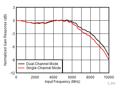
 ADC12DLx500 Frequency Response