SBASAT9 February 2024 ADC12DL1500 , ADC12DL2500 , ADC12DL500
PRODUCTION DATA
- 1
- 1 Features
- 2 Applications
- 3 Description
- 4 Pin Configuration and Functions
-
5 Specifications
- 5.1 Absolute Maximum Ratings
- 5.2 ESD Ratings
- 5.3 Recommended Operating Conditions
- 5.4 Thermal Information
- 5.5 Electrical Characteristics: DC Specifications
- 5.6 Electrical Characteristics: Power Consumption
- 5.7 Electrical Characteristics: AC Specifications (Dual-Channel Mode)
- 5.8 Electrical Characteristics: AC Specifications (Single-Channel Mode)
- 5.9 Timing Requirements
- 5.10 Switching Characteristics
- 5.11 Timing Diagrams
- 5.12 Typical Characteristics - ADC12DL500
- 5.13 Typical Characteristics - ADC12DL1500 (1GSPS)
- 5.14 Typical Characteristics - ADC12DL1500 (1.5GSPS)
- 5.15 Typical Characteristics - ADC12DL2500 (2GSPS)
- 5.16 Typical Characteristics - ADC12DL2500 (2.5GSPS)
-
6 Detailed Description
- 6.1 Overview
- 6.2 Functional Block Diagram
- 6.3
Feature Description
- 6.3.1 Analog Inputs
- 6.3.2 ADC Core
- 6.3.3 Timestamp
- 6.3.4 Clocking
- 6.3.5 LVDS Digital Interface
- 6.3.6 Alarm Monitoring
- 6.3.7 Temperature Monitoring Diode
- 6.3.8 Analog Reference Voltage
- 6.4
Device Functional Modes
- 6.4.1 Dual-Channel Mode (Non-DES Mode)
- 6.4.2 Internal Dither Modes
- 6.4.3 Single-Channel Mode (DES Mode)
- 6.4.4 LVDS Output Driver Modes
- 6.4.5 LVDS Output Modes
- 6.4.6 Power-Down Modes
- 6.4.7 Calibration Modes and Trimming
- 6.4.8 Offset Calibration
- 6.4.9 Trimming
- 6.5 Programming
- 7 Application and Implementation
- 8 Register Maps
- 9 Device and Documentation Support
- 10Revision History
- 11Mechanical, Packaging, and Orderable Information
Package Options
Mechanical Data (Package|Pins)
- ACF|256
Thermal pad, mechanical data (Package|Pins)
Orderable Information
7.4 Power Supply Recommendations
The device requires two different power-supply voltages. 1.9V DC is required for the VA19 power bus and 1.1V DC is required for the VA11 and VD11 power buses. VLVDS can be set to any voltage between 1.9V and 1.1V. The LVDS output driver common-mode voltage tracks the VLVDS supply voltage. In general, a 1.9V supply voltage for VLVDS can be used for standard LVDS receivers.
The power-supply voltages must be low noise and provide the needed current to achieve rated device performance.
| DEVICE POWER SUPPLY | SUPPLY VOLTAGE | CURRENT REQUIREMENT |
|---|---|---|
| VA19 | 1.9V | 1A |
| VA11 | 1.1V | 600mA |
| VD11 | 1.1V | 300mA |
| VLVDS | 1.1-1.9V | 500mA |
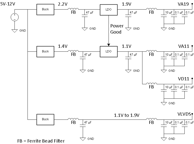
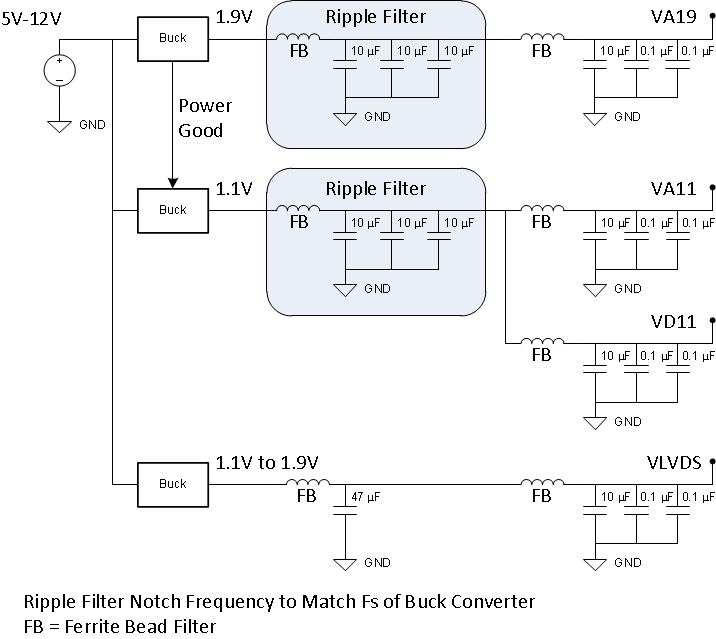
There are two recommended power-supply architectures:
- Step down using high-efficiency switching converters, followed by a second stage of regulation to provide switching noise reduction and improved voltage accuracy.
- Directly step down the final ADC supply voltage using high-efficiency switching converters. This approach provides the best efficiency, but care must be taken to ensure switching noise is minimized to prevent degraded ADC performance.
TI WEBENCH® Power Designer can be used to select and design the individual power-supply elements needed: see the WEBENCH® Power Designer
Recommended switching regulators for the first stage include the TPS62085, TPS82130, TPS62130A, and similar devices.
Recommended low dropout (LDO) linear regulators include the TPS7A7200, TPS74401, and similar devices.
For the switcher only approach, the ripple filter must be designed with a notch frequency that aligns with the switching ripple frequency of the DC/DC converter. Make a note of the switching frequency reported from WEBENCH® and design the EMI filter and capacitor combination to have the notch frequency centered as needed. Figure 7-10 and Figure 7-11 illustrate the two approaches. Do not share VLVDS with the analog supply voltages in order to prevent digital switching noise from coupling into the analog signal chain. If VLVDS must be shared with either VA11 or VA19, apply careful power supply filtering to limit digital noise at the analog supply pins.

