The ADC16DX370 device is a monolithic dual-channel high performance analog-to-digital converter capable of converting analog input signals into 16-bit digital words with a sampling rate of 370 MSPS. This converter uses a differential pipelined architecture with integrated input buffer to provide excellent dynamic performance while maintaining low power consumption.
The integrated input buffer eliminates charge kickback noise coming from the internal switched capacitor sampling circuits and eases the system-level design of the driving amplifier, anti-aliasing filter, and impedance matching. An input sampling clock divider provides integer divide ratios with configurable phase selection to simplify system clocking. An integrated low-noise voltage reference eases board level design without requiring external decoupling capacitors. The output digital data is provided through a JESD204B subclass 1 interface from a 56-pin, 8-mm × 8-mm WQFN package. A SPI is available to configure the device that is compatible with 1.2-V to 3-V logic.
PART NUMBER | PACKAGE | BODY SIZE (NOM) |
---|---|---|
ADC16DX370 | WQFN (56) | 8.00 × 8.00 mm |
SPACE
Changes from B Revision (April 2014) to C Revision
Changes from A Revision (April 2014) to B Revision
Changes from * Revision (April 2014) to A Revision
PIN | TYPE OR DIAGRAM | DESCRIPTION | |
---|---|---|---|
NAME | NUMBER | ||
AGND | 3, 6, 9, 12, 16, 19, 22, 31, 40, 49, 52, 55 | Analog ground | Analog ground Must be connected to a solid ground reference plane under the device. |
BP2.5 | 41 | Bypass pins | Capacitive bypassing pin for internally regulated 2.5-V supply This pin must be decoupled to AGND with a 0.1-μF and a 10-µF capacitor located close to the pin. |
CLKIN+, CLKIN– | 17, 18 |
![]() |
Differential device clock input pins Each pin is internally terminated to a DC bias with a 50-Ω resistor for a 100-Ω total internal differential termination. AC coupling is required for coupling the clock input to these pins if the clock driver cannot meet the common-mode requirements. Sampling occurs on the rising edge of the differential signal (CLKIN+) − (CLKIN–). |
CSB | 54 |
![]() |
SPI chip select pin When this signal is asserted, SCLK is used to clock the input serial data on the SDI pin or output serial data on the SDO pin. When this signal is de-asserted, the SDO pin is high impedance and the input data is ignored. Active low. A 10 kΩ pull-up resistor to the VA1.8 supply is recommended to prevent undesired activation of the SPI bus. Compatible with 1.2- to 3.0-V CMOS logic levels. |
DGND | 25, 46 | Digital ground | Digital ground Must be connected to the same solid ground reference plane under the device to which AGND connects. Bypass capacitors connected to the VD1.2 pins must be connected to ground as close to this DGND pins as possible. |
OVRA, OVRB | 44, 43 |
![]() |
Over-range detection outputs These pins output the channel A and channel B over-range signals as 1.8-V CMOS logic level outputs. |
SA0+, SA0–, SA1+, SA1– | 38, 39, 36, 37 |
![]() |
Differential high speed serial data lane pins for channel A These pins must be AC coupled to the receiving device. The differential trace routing from these pins must maintain a 100-Ω characteristic impedance. In single-lane mode, SA0+ or SAO– is used to transfer data and SA1+ or SA1– is undefined and may be left floating. |
SB0+, SB0–, SB1+, SB1– | 32, 33, 34, 35 | Differential high speed serial data lane pins for channel B. These pins must be AC coupled to the receiving device. The differential trace routing from these pins must maintain a 100-Ω characteristic impedance. In single-lane mode, SB0+ or SB0– is used to transfer data and SB1+ and SB1– is undefined and may be left floating. | |
SCLK | 53 |
![]() |
SPI serial clock pin Serial data is shifted into and out of the device synchronous with this clock signal. Compatible with 1.2- to 3.0-V CMOS logic levels. |
SDI | 47 | SPI data input pin Serial data is shifted into the device on this pin while the CSB signal is asserted. Compatible with 1.2- to 3.0-V CMOS logic levels. |
|
SDO | 48 |
![]() |
SPI data output pin Serial data is shifted out of the device on this pin during a read command while CSB is asserted. The output logic level is configurable as 1.2, 1.8, 2.5, or 3.0 V. The output level must be configured after power up and before performing a read command. See the Register Descriptions for configuration details. |
SYNCb+, SYNCb– | 27, 28 |
![]() |
Differential SYNCb signal input pins DC coupling is required for coupling the SYNCb signal to these pins. Each pin is internally terminated to the DC bias with a large resistor. An internal 100-Ω differential termination is provided therefore an external termination is not required. Additional resistive components in the input structure give the SYNCb input a wide input common-mode range. The SYNCb signal is active low and therefore asserted when the voltage at SYNCb+ is less than at SYNCb–. |
SYSREF+, SYSREF– | 23, 24 |
![]() |
Differential SYSREF signal input pins Each pin is internally terminated to a DC bias with a 1-kΩ resistor. An external 100-Ω differential termination must always be provided. AC coupling using capacitors is required for coupling the SYSREF signal to these pins if the clock driver cannot meet the common-mode requirements. In the case of AC coupling, the termination must be placed on the source side of the coupling capacitors. |
VA1.2 | 8, 21, 30, 50 | Supply input pin | 1.2-V analog power supply pins These pins must be connected to a quiet source and decoupled to AGND with a 0.1-μF and 0.01-μF capacitor located close to each pin. |
VA1.8 | 7, 15, 20, 29, 51, 56 | Supply input pin | 1.8-V analog power supply pins These pins must be connected to a quiet source and decoupled to AGND with a 0.1-μF and 0.01-μF capacitor located close to each pin. |
VA3.0 | 2, 13, 42 | Supply input pin | 3.0-V analog power supply pin This pin must be connected to a quiet source and decoupled to AGND with a 0.1-μF and 0.01-μF capacitor located close to the pin. |
VCMA, VCMB | 1, 14 |
![]() |
Input interface common mode voltage for channels A and B These pins must be bypassed to AGND with low equivalent series inductance (ESL) 0.1-μF capacitors. One capacitor should be placed as close to the pin as possible and additional capacitors placed at the bias load points. 10-μF capacitors should also be placed in parallel. TI recommends to use VCMA and VCMB to provide the common mode voltage for the differential analog inputs. The input common mode bias is provided internally for the ADC input; therefore, external use of VCMA and VCMB is recommended, but not strictly required. The recommended bypass capacitors are always required. |
VD1.2 | 26, 45 | Supply input pin | 1.2-V digital power supply pin This pin must be connected to a quiet source and decoupled to AGND with a 0.1-μF and 0.01-μF capacitor located close to each pin. |
VINA+, VINA– | 4, 5 |
![]() |
Differential analog input pins of channel A Each input pin is terminated to the internal common mode reference with a resistor for an internal differential termination. |
VINB+, VINB– | 11, 10 | Differential analog input pins of channel B Each input pin is terminated to the internal common mode reference with a resistor for an internal differential termination. |
|
0 | Exposed thermal pad | Exposed thermal pad The exposed pad must be connected to the AGND ground plane electrically and with good thermal dissipation properties to achieve rated performance. |
MIN | MAX | UNIT | ||
---|---|---|---|---|
Supply Voltage: VA3.0 | –0.3 | 4.2 | V | |
Supply Voltage: VA1.8 | –0.3 | 2.35 | V | |
Supply Voltage: VA1.2, VD1.2 | –0.3 | 1.55 | V | |
Voltage at VINA+, VINA– | VCMA – 1.0 | VCMA + 0.75 | V | |
Voltage at VINB+, VINB– | VCMB – 1.0 | VCMB + 0.75 | V | |
Voltage at VCMA, VCMB | –0.3 | VA3.0 + 0.3, not to exceed 4.2 V | V | |
Voltage at OVRA, ORVB | –0.3 | VA1.8 + 0.3 | V | |
Voltage at SCLK, SDI, CSb | –0.3 | VA3.0 + 0.3, not to exceed 4.2 V | V | |
Voltage at SDO | –0.3 | VSPI + 0.3, not to exceed 4.2 V | V | |
Voltage at CLKIN+, CLKIN–, SYSREF+, SYSREF– | –0.3 | 1.55 | V | |
Voltage at SYNC+, SYNC– | –0.3 | VBP2.5 + 0.3 | V | |
Voltage at BP2.5 | –0.3 | 3.2 | V | |
Voltage at SA0+, SA0–, SA1+, SA1–, SB0+, SB0–, SB1+, SB1– | –0.3 | VBP2.5 + 0.3 | V | |
Input current at any pin(3) | 5 | mA | ||
TJ | Operating junction temperature(2) | 125 | °C |
MIN | MAX | UNIT | |||
---|---|---|---|---|---|
Tstg | Storage temperature range | –65 | 150 | °C | |
V(ESD)(1) | Electrostatic discharge | Human body model (HBM), per ANSI/ESDA/JEDEC JS-001, all pins(2) | –1000 | 1000 | V |
Charged device model (CDM), per JEDEC specification JESD22-C101, all pins(3) | –250 | 250 | V |
MIN | MAX | UNIT | ||
---|---|---|---|---|
Specified temperature | –40 | 85 | °C | |
VA3.0 | 3.0-V analog supply voltage | 2.85 | 3.45 | V |
VA1.8 | 1.8-V analog supply voltage | 1.7 | 1.9 | V |
VA1.2 | 1.2-V analog supply voltage | 1.15 | 1.25 | V |
VD1.2 | 1.2-V digital supply voltage | 1.15 | 1.25 | V |
CLKIN duty cycle | 30% | 70% | ||
TJ | Operating junction temperature | 105 | °C |
THERMAL METRIC(1) | WQFN (56 PINS) | UNIT | |
---|---|---|---|
RθJA | Thermal resistance, junction to ambient | 24.9 | °C/W |
RθJC(top) | Thermal resistance, junction to package top | 8.6 | |
RθJB | Thermal resistance, junction to board | 3.0 | |
φJT | Characterization parameter, junction to package top | 0.2 | |
φJB | Characterization parameter, junction to board | 2.9 |
PARAMETER | TEST CONDITIONS | MIN | TYP | MAX | UNIT | ||
---|---|---|---|---|---|---|---|
IA3.0 | VA3.0 supply current consumption | Normal operation, single data lane per channel | 230 | mA | |||
Normal operation, dual data lane per channel | 255 | ||||||
Power down mode | 8.7 | ||||||
IA1.8 | VA1.8 supply current consumption | Normal operation | 360 | mA | |||
Power down mode | 3.6 | ||||||
IA1.2 | VA1.2 supply current consumption | Normal operation | 172 | mA | |||
Power down mode | 3.3 | ||||||
ID1.2 | VD1.2 supply current consumption | Normal operation | 52 | mA | |||
Power down mode | 3.3 | ||||||
PT | Total power consumption of the VA3.0 , VA1.8 , VA1.2 , VD1.2 supplies |
Normal operation, single serial lane per channel | TA = 25°C | 1607 | mW | ||
TA = TMIN to TMAX | 1800 | ||||||
Power consumption during power-down state, external clock active | 30 | ||||||
Power consumption during sleep state, external clock active | 30 | ||||||
VBP2.5 | Voltage at the BP2.5 pin | 2.65 | V | ||||
Supply sensitivity to noise Power of spectral spur resulting from a 100-mV sinusoidal signal modulating a supply at 500 kHz. Analog input is a –3 dBFS 150-MHz single tone. In all cases, the spur appears as part of a pair symmetric about the fundamental that scales proportionally with the fundamental amplitude. |
dBFS | ||||||
VA3.0 | –72.5 | ||||||
VA1.8 | –58.0 | ||||||
VA1.2 | –37.7 | ||||||
VD1.2 | –78 |
PARAMETER | DESCRIPTION AND TEST CONDITIONS | MIN | TYP | MAX | UNIT | ||
---|---|---|---|---|---|---|---|
FSR | Full scale range Differential peak-to-peak |
1.7 | Vpp | ||||
GVAR | Gain variation Variation of input voltage to output code gain between different parts, part-to-part or channel-to-channel |
±0.07 | dB | ||||
VOFF | Input referred voltage offset | ±13 | mV | ||||
BW3dB | 3-dB bandwidth Frequency at which the voltage input to digital output response deviates by 3 dB compared to low frequencies for a low impedance differential signal applied at the input pins. Includes 0.5-nH parasitic inductance in series with each pin of the differential analog input. |
800 | MHz | ||||
RIN | Input termination resistance Differential |
200 | Ω | ||||
CIN | Input capacitance, differential | 3.7 | pF | ||||
VCMA, VCMB | Input common mode voltage reference voltage at the VCMA or VCMB pins Varies with temperature |
1.6 | V | ||||
IVCM | Input common mode voltage reference current sourcing or sinking on VCMA or VCMB pins | 1 | mA | ||||
VCM-OFF | Input common mode voltage offset range Allowable difference between the common mode applied to the analog input of a particular channel and the bias voltage at the respective common mode VCM bias pin (VCMA or VCMB) |
±50 | mV |
PARAMETER | DESCRIPTION AND TEST CONDITIONS | MIN | TYP | MAX | UNIT | |
---|---|---|---|---|---|---|
DIGITAL INPUT CHARACTERISTICS (CLKIN) | ||||||
VID | Input differential voltage(1)(3)
Differential peak voltage |
250 | 1000 | mV | ||
dVSS/dt | Recommended minimum edge slew rate at the zero crossing(1)
|
2 | 5 | V/ns | ||
VIS-BIAS | Input offset voltage internal bias (1)
Internally biased |
0.5 | V | |||
VIS-IN | Externally applied input offset voltage(3)
Allowable common mode voltage range for DC coupled interfaces |
0.4 | 0.5 | 0.6 | V | |
Zrdiff | Differential termination resistance at DC(2) | 130 | Ω | |||
Ztt | Common-mode bias source impedance(2) | 11 | kΩ | |||
CT | Differential termination capacitance | 1.5 | pF | |||
DIGITAL INPUT CHARACTERISTICS (SYSREF) | ||||||
VID | Input differential voltage (1)(3)
Differential peak voltage |
250 | 1000 | mV | ||
VIS-BIAS | Input offset voltage bias (1)
Internally biased |
0.5 | V | |||
VIS-IN | Externally applied input offset voltage(3)
Allowable common mode voltage range for DC coupled interfaces |
0.4 | 0.5 | 0.6 | V | |
Zrdiff | Differential termination resistance at DC(2) | 2 | kΩ | |||
Ztt | Common-mode bias source impedance(2) | 11 | kΩ | |||
CT | Differential termination capacitance(2) | 0.8 | pF | |||
DIGITAL INPUT CHARACTERISTICS (SYNCb) | ||||||
VID | Input differential voltage (1)(3)
Differential peak voltage |
350 | mV | |||
VIS-IN | Externally applied input offset voltage(1)(3) | 0.5 | 1.2 | 2 | V | |
Zrdiff | Differential termination resistance(2) | 100 | Ω | |||
CT | Differential termination capacitance(2) | 1 | pF |
PARAMETER | DESCRIPTION AND TEST CONDITIONS | MIN | TYP | MAX | UNIT | |
---|---|---|---|---|---|---|
SERIAL LANE OUTPUT CHARACTERISTICS (SA0, SA1, SB0, SB1) | ||||||
VOD | Output differential voltage(1)
Differential peak-peak values. Assumes ideal 100-Ω load. De-emphasis disabled. Configurable via SPI |
580 680 760 860 960 1060 1140 1240 |
mV | |||
Zddiff | Differential output impedance at DC(2) | 100 | Ω | |||
RLddiff | Differential output return loss magnitude Relative to 100 Ω; For frequencies up to 5.5 GHz |
–11 | dB | |||
Rdeemp | Transmitter de-emphasis values VOD configured to default value. |
0 0.4 1.2 2.1 2.8 3.8 4.8 6.8 |
dB |
PARAMETER | DESCRIPTION AND TEST CONDITIONS | MIN | TYP | MAX | UNIT | |
---|---|---|---|---|---|---|
DIGITAL INPUT CHARACTERISTICS (SDI, SCLK, CSB) | ||||||
VIH | Logical 1 input voltage(1)
Inputs are compatible with 1.2-V up to 3.0-V logic. |
0.9 | V | |||
VIL | Logical 0 input voltage(1) | 0.3 | V | |||
IIN0 | Logic low input current | 0.5 | uA | |||
IIN1 | Logic high input current | 0.5 | uA | |||
CIN | Input capacitance | 2 | pF | |||
DIGITAL OUTPUT CHARACTERISTICS (SDO) | ||||||
VOH | Logical 1 output voltage(1)(2)
VSPI = 1.2, 1.8, 2.5, or 3 V ; Configurable via SPI |
VSPI – 0.3 | VSPI(2) | V | ||
VOL | Logical 0 output voltage(1)(2) | 0 | 0.3 | V | ||
+ISC | Logic high short circuit current | 9 | mA | |||
–ISC | Logic low short circuit current | –10 | mA | |||
DIGITAL OUTPUT CHARACTERISTICS (OVRA/TRIGRDY, OVRB) | ||||||
VOH | Logical 1 output voltage(1) | 1.5 | 1.8 | V | ||
VOL | Logical 0 output voltage(1) | 0 | 0.3 | V | ||
+ISC | Logic high short circuit current | 17.7 | mA | |||
–ISC | Logic low short circuit current | –15 | mA | |||
DIGITAL INPUT CHARACTERISTICS (TRIGGER) | ||||||
VIH | Logical 1 input voltage(1) | 1.5 | V | |||
VIL | Logical 0 input voltage(1) | 0.3 | V | |||
IIN0 | Logic low input current | 0.5 | uA | |||
IIN1 | Logic high input current | 0.5 | uA | |||
CIN | Input capacitance | 3 | pF |
PARAMETER | DESCRIPTION | MIN | TYP | MAX | UNIT | |
---|---|---|---|---|---|---|
ADC SAMPLING INSTANT TIMING CHARACTERISTICS | ||||||
FS | Sampling rate Equal to FCLKIN / CLKDIV |
50 | 370 | MSPS | ||
FCLKIN | Input Clock Frequency at CLKIN Inputs | MHz | ||||
CLKDIV = 1 | 50 | 370 | ||||
CLKDIV = 2 | 100 | 740 | ||||
CLKDIV = 4 | 200 | 1480 | ||||
CLKDIV = 8 | 400 | 2000 | ||||
tLAT-ADC | ADC core latency Delay from a reference sampling instant to the boundary of the internal LMFC where the reference sample is the first sample of the next transmitted multi-frame. Coarse sampling phase adjust disabled. In this device, the frame clock period is equal to the sampling clock period. |
12.5 | Frame clock cycles | |||
tJ | Additive sampling aperture jitter Depends on input CLKIN differential edge rate at the zero crossing, dVSS/dt. Tested with 5 V/ns edge rate. |
fs | ||||
CLKDIV = 1 | 70 | |||||
CLKDIV = 2, 4, coarse phase disabled | 80 | |||||
CLKDIV = 4, coarse phase enabled. Typical worst-case value across all coarse phase configuration possibilities. | 85 | |||||
OVER-RANGE INTERFACE TIMING CHARACTERISTICS (OVRA, OVRB) | ||||||
tODH | OVR assertion delay Delay between an over-range value sampled and OVR asserted; Coarse clock phase adjust disabled. |
7.5 | Frame clock cycles | |||
tODL | OVR de-assertion delay Delay between first under-range value sampled until OVR de-assertion; Configurable via SPI. |
tODH + 0 | tODH + 15 | Frame clock cycles | ||
SYSREF TIMING CHARACTERISTICS | ||||||
tPH-SYS | SYSREF assertion duration Required duration of SYSREF assertion after rising edge event |
2 | Frame clock cycles | |||
tPL-SYS | SYSREF de-assertion duration Required duration of SYSREF de-assertion after falling edge event |
2 | Frame clock cycles | |||
tS-SYS | SYSREF setup time Relative to CLKIN rising edge |
320 | ps | |||
tH-SYS | SYSREF hold time Relative to CLKIN rising edge |
80 | ps | |||
JESD204B INTERFACE LINK TIMING CHARACTERISTICS | ||||||
tD-LMFC | SYSREF to LMFC delay Functional delay between SYSREF assertion latched and LMFC frame boundary. Depends on CLKDIV setting. |
CLKIN cycles (Frame clock cycles) |
||||
CLKDIV = 1 | 3.5 (3.5) |
|||||
CLKDIV = 2 | 8 (4) |
|||||
CLKDIV = 4 | 15 (3.75) |
|||||
CLKDIV = 8 | 29 (3.625) |
|||||
tD-K28 | LMFC to K28.5 delay Functional delay between the start of the first K28.5 frame during Code Group Synchronization at the serial output and the preceding LMFC frame boundary. |
5 | 6 | 7 | Frame clock cycles | |
tD-ILA | LMFC to ILA delay Functional delay between the start of the first ILA frame during Initial Lane Synchronization at the serial output and the preceding LMFC frame boundary |
5 | 6 | 7 | ||
tD-DATA | LMFC to valid data delay Functional delay between the start of the first valid data frame at the serial output and the preceding LMFC frame boundary. |
5 | 6 | 7 | ||
tS-SYNCb-F | SYNCb setup time Required SYNCb setup time relative to the internal LMFC boundary. |
3 | Frame clock cycles | |||
tH-SYNCb-F | SYNCb hold time Required SYNCb hold time relative to the internal LMFC boundary . |
0 | ||||
tH-SYNCb | SYNCb assertion hold time Required SYNCb hold time after assertion before de-assertion to initiate a link re-synchronization. |
4 | ||||
tILA | ILA duration Duration of the ILA sequence . |
4 | Multi-frame clock cycles | |||
SERIAL OUTPUT DATA TIMING CHARACTERISTICS | ||||||
FSR | Serial bit rate Single- or dual-lane mode |
1 | 7.4 | Gb/s | ||
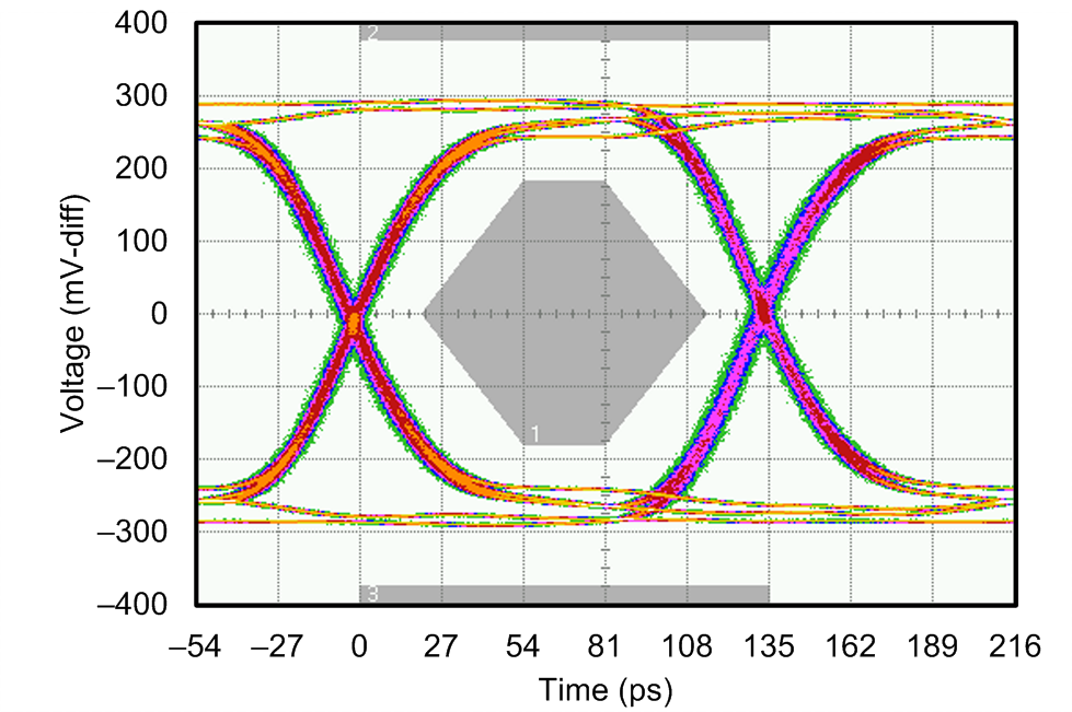
UI | Unit Interval 7.4 Gb/s Data Rate |
135.1 | ps | |||
DJ | Deterministic jitter Includes periodic jitter (PJ), data dependent jitter (DDJ), duty cycle distortion (DCD), and inter-symbol interference (ISI); 7.4 Gb/s data rate. |
0.047 (6.33) |
p-p UI (p-p ps) |
|||
RJ | Random jitter Assumes BER of 1e-15 (Q = 15.88); 7.4 Gb/s data rate |
0.156 (1.35) |
p-p UI (rms ps) |
|||
TJ | Total jitter Sum of DJ and RJ. Assumes BER of 1e-15 (Q = 15.88); 7.4 Gb/s data rate. |
0.206 (27.77) |
p-p UI (p-p ps) |
|||
SPI BUS TIMING CHARACTERISTICS(1) | ||||||
ƒSCLK | Serial clock frequency fSCLK = 1 / tP |
20 | MHz | |||
tPH | SCLK pulse width – high % of SCLK period |
25% | 75% | |||
tPL | SCLK pulse width – low % of SCLK period |
25% | 75% | |||
tSSU | SDI input data setup time | 5 | ns | |||
tSH | SDI input data hold time | 5 | ns | |||
tODZ | SDO output data driven-to-3-state time | 25 | ns | |||
tOZD | SDO output data 3-state-to-driven time | 25 | ns | |||
tOD | SDO output data delay time | 30 | ns | |||
tCSS | CSB setup time | 5 | ns | |||
tCSH | CSB hold time | 5 | ns | |||
tIAG | Inter-access gap Minimum time CSB must be de-asserted between accesses |
5 | ns |
For more information, see Functional Block Diagram.
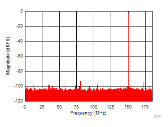
SNR = 68.49 dBFS | SFDR = 83.21 dBFS | |
Nominal Supplies: | VA3.0 = 3.0 V | VA1.2 = VD1.2 = 1.2 V |
VA1.8 = 1.8 V |
Nominal Supplies: | VA3.0 = 3.0 V | VA1.2 = VD1.2 = 1.2 V |
VA1.8 = 1.8 V |
SNR = 69.5 dBFS | SFDR = 87.0 dBFS |
SNR = 69.5 dBFS | SFDR = 94 dBFS | IMD3 = –100 dBFS |
Unless otherwise noted, these specifications apply for all supply and temperature conditions.
PARAMETER | DESCRIPTION AND TEST CONDITIONS | VALUE | UNIT | |
---|---|---|---|---|
OVRTH | Over-range detection threshold Configurable via SPI |
–48.16 (min) and 0 (max) | dBFS | |
OVRTHS | Over-range detection threshold step Expressed as the change in the total code range outside of which an over-range event occurs. Half of the step value is changed at the upper boundary of the code range and half is changed at the lower boundary. |
256 | codes |
Unless otherwise noted, these specifications apply for VA3.0 = 3.0 V; VA1.8 = 1.8 V; VA1.2 = VD1.2 = 1.2 V; FCLKIN = FS = 370 MSPS. Typical values are at TA = +25°C.
PARAMETER | DESCRIPTION AND TEST CONDITIONS | TYP | LIMIT | UNIT | |
---|---|---|---|---|---|
CLKDIV | Input CLKIN divider factor Configurable via SPI |
1 (default), 2, 4, or 8 | |||
NФC | Number of available coarse phase adjustment steps | 2 × CLKDIV | |||
ФC | Nominal CLKIN coarse phase adjustment step Coarse step of CLKIN divider phase adjustment range; common to both channels; depends on clock divider factor (CLKDIV) and sampling rate (FS). |
1 / (2 × CLKDIV × FS) | s | ||
ΔФC | Typical coarse phase adjustment step error(1)
Percent variation of actual phase adjustment step relative to the nominal step (ФC). Assumes ideal 50% CLKIN duty cycle |
||||
CLKDIV = 8, FS = 250 MSPS | ±6% | ||||
CLKDIV = 4, FS = 370 MSPS | ±4% |
Unless otherwise noted, these specifications apply for all supply and temperature conditions.
PARAMETER | DESCRIPTION AND TEST CONDITIONS | VALUE | |
---|---|---|---|
LSF | Supported configurations L = Number of lanes/converter S = Samples per frame F = Octets per frame |
L = 1, S = 1, F = 2 or L = 2, S = 1, F = 1 |
|
K | Number of frames per multi-frame Configurable via SPI |
||
L = 1, S = 1, F = 2 | 9 (min) 32 (max, default) |
||
L = 2, S = 1, F = 1 | 17 (min) 32 (max, default) |
The ADC16DX370 device is a dual analog-to-digital converter (ADC) composed of pipelined stages followed by a back-end JESD204B interface. Each ADC core is preceded by an input buffer and imbalance correction circuit at the analog input and is provided with the necessary reference voltages with internal drivers that require no external components. The analog input common-mode is also internally regulated.
Over-range signals are externally available on pins to monitor the signal path. A DC offset correction block is disabled by default, but may also be enabled at the ADC core output to remove DC offset. Processed data is passed into the JESD204B interface where the data is framed, encoded, serialized, and output on one or two lanes per channel. Data is serially transmitted by configurable high-speed voltage mode drivers.
The sampling clock is derived from the CLKIN input via a low-noise receiver and clock divider. Coarse delay adjustment blocks in the clock signal path control the phase of the sampling instant. The CLKIN, SYSREF, and SYNCb inputs provide the device clock, sysref, and sync~ signals to the JESD204B interface, which are used to derive the internal local frame and local multi-frame clocks and establish the serial link.
Features of the ADC16DX370 device are configurable through the 4-wire SPI.
The ADC performance can be sensitive to amplitude and phase imbalance of the input differential signal and therefore integrates a front-end balance correction circuit to optimize the second-order distortion (HD2) performance of the ADC in the presence of an imbalanced input signal. 4-bit control of the phase mismatch and 3-bit control of the amplitude mismatch corrects the input mismatch before the input buffer. A simplified diagram of the amplitude and phase correction circuit at the ADC input is shown in Figure 30.
Amplitude correction is achieved by varying the single-ended termination resistance of each input while maintaining constant total differential resistance, thereby adjusting the amplitude at each input but leaving the differential swing constant. Phase correction, also considered capacitive balance correction, varies the capacitive load at the ADC input, thereby correcting a phase imbalance by creating a bandwidth difference between the analog inputs that minimally affects amplitude. This function is useful for correcting the balance of transformers or filters that drive the ADC analog inputs. Figure 31 shows the measured HD2 resulting from an example 250-MHz imbalanced signal input into the ADC16DX370 device recorded over the available amplitude and phase correction settings, demonstrating the optimization of HD2. Performance parameters in the Converter Performance Characteristics are characterized with the amplitude and phase correction settings in the default condition.
DC offset correction is provided using a digital high-pass IIR filter at the immediate output of the ADC core. The DC offset correction is bypassed by default, but may be enabled and configured via the SPI. The 3-dB bandwidth of the IIR digital correction filter may be set to four different low-frequency values. When DC offset correction is enabled, any signal in the stop-band of the high-pass filter is attenuated. The settling time of the DC offset correction is approximately equal to the inverse of the 3-dB bandwidth setting.
Separate over-range detection output signals for channels A and B are dedicated to pins. The OVRA pin asserts (high) when an over-range signal is detected at the input of channel A. The short delay from when an over-range signal is incident at the input until the OVRA is asserted allows for almost immediate detection of over-range signals without delay from the internal ADC pipeline latency or data serialization latency. OVRB responds similarly when an over-range signal is detected at the input of channel B.
The input power threshold to indicate an over-range event is programmable via the SPI from full scale code range down to a ± 128 LSB code range in steps of 128 codes relative to the 16-bit code range of the data at the output of the ADC core.
After an over-range event occurs and the signal at the channel input reduces to a level below full-scale, an internal counter begins counting to provide a hold function. When the counter reaches a programmable counter threshold, the OVRA (or OVRB) signal is de-asserted. The duration of the hold counter is programmable via the SPI to hold for +3, +7, or +15 frame clock cycles. The counter is disabled (+0 cycles) by default to allow de-assertion without holding. Each channel has an independent hold counter but the hold duration value is common to both channels.
An input clock divider allows a high frequency clock signal to be distributed throughout the system and locally divided down at the ADC device so that coupling of signals at common intermediate frequencies into other parts of the system can be avoided. The frequency at the CLKIN input may be divided down to the sampling rate of the ADC by factors of 1, 2, 4, or 8. Changing the clock divider setting initiates a JESD204 link re-initialization and requires re-calibration of the ADC if the sampling rate is changed from the rate during the previous calibration.
When the signal at the SYSREF input is not actively toggling periodically, the SYSREF signal is considered to be in an idle state. The idle state is recommended at any time the ADC16DX370 spurious performance must be maximized. When the SYSREF signal is in the idle state for longer than 1 µs, an undesirable offset voltage may build up across the AC coupling capacitors between the SYSREF transmitter and the ADC16DX370 device input. This offset voltage creates a signal threshold problem, requires a long time to dissipate, and therefore prevents quick transition of the SYSREF signal out of the idle state. Two features are provided as a solution and are shown in Figure 48, namely the SYSREF offset feature and SYSREF detection gate.
In the case that the SYSREF signal idle state has a 0-V differential value, or if the ADC16DX370 device must be insensitive to noise that may appear on the SYSREF signal, then the SYSREF detection gate may be used. The detection gate is the AND gate shown in Figure 48 that enables or disables propagation of the SYSREF signal through to the internal device logic. If the detection gate is disabled and a false edge appears at the SYSREF input, the signal does not disrupt the internal clock alignment. Note that the SYSREF detection gate is disabled by default; therefore, the device does not respond to a SYSREF edge until the detection gate is enabled.
The SYSREF offset and detection gate features are both controlled through the SPI.
Adjustment of the ADC sampling instant relative to the CLKIN input clock may be controlled using the coarse phase adjustment feature.
Coarse clock phase adjustment is provided to control the phase of the sampling instant in the ADC cores. The coarse phase steps are equal to 1 / (2 × CLKDIV × FS) seconds over a 1 / FS second range where CLKDIV is the clock division factor and FS is the sampling rate. The coarse phase adjustment setting is common to both channels.
Affter the JESD204B serial link is established, the frame and LMFC clocks, as well as the internal reference clocks used by the JESD204B serializer, are not affected by the clock phase adjustments because the data is re-timed at the ADC core output. Changing the phase setting does not affect the status of the JESD204B link and does not cause glitches in the serial data. Varying the phase does not vary the timing of frames output on the JESD204B link, but it does vary the sampling instant relative to the internal frame clock. Therefore, the total latency from the sampling instant to the beginning of the frame output on the serial link changes equal to the change in the phase adjustment. This latency change is a fraction of a frame clock cycle.
The phase of the internal sampling clock is aligned to SYSREF events. This impacts the phase relationship between the input signal and sampling instant and may affect the latency across the link.
The differential drivers of the ADC16DX370 device that output the serial JESD204B data are voltage mode drivers with amplitude control and de-emphasis features that may be configured through the SPI for a variety of different channel applications. Eight amplitude control (VOD) and eight de-emphasis control (DEM) settings are available. Both VOD and DEM register fields must be configured to optimize the noise performance of the serial interface for a particular lossy channel.
The output common-mode of the driver varies with the configuration of the output swing. Therefore, AC coupling is strongly recommended between the ADC16DX370 device and the device receiving the serial data.
De-emphasis of the differential output is provided as a form of continuous-time linear equalization that imposes a high-pass frequency response onto the output signal to compensate for frequency-dependent attenuation as the signal propagates through the channel to the receiver. In the time-domain, the de-emphasis appears as the bit transition transient followed by an immediate reduction in the differential amplitude, as shown in Figure 32. The characteristic appearance of the waveform changes with differential amplitude and the magnitude of de-emphasis applied. The serial lane rate determines the available period of time during which the de-emphasis transient settles. However, the lane rate does not affect the settling behavior of the applied de-emphasis.
Table 1 indicates the typical measured values for the de-emphasis range, where the de-emphasis value is measured as the ratio (in units of [dB]) between the peak voltage after the signal transition to the settled voltage value in one bit period. The data rate for this measurement is 1.2 Gb/s to allow settling of the de-emphasis transient. Table 1 illustrates the actual de-emphasis value in terms of voltage attenuation and shows dependence on the amplitude setting, but does not reflect the optimal amplitude setting (VOD) and de-emphasis setting (DEM) for a particular lossy channel. Table 2 shows the amplitude of the differential signal swing during its settled state after the transition transient. The measurement is performed at 1.2 Gb/s and the units are in differential peak-to-peak mV.
DEM | |||||||||
---|---|---|---|---|---|---|---|---|---|
0 | 1 | 2 | 3 | 4 | 5 | 6 | 7 | ||
VOD | 0 | 0 | –0.4 | –1.2 | –2.1 | –2.8 | –3.8 | –4.8 | –6.8 |
1 | 0 | –0.6 | –1.7 | –2.7 | –3.5 | –4.6 | –5.7 | –7.8 | |
2 | 0 | –0.8 | –2.2 | –3.3 | –4.1 | –5.3 | –6.4 | –8.6 | |
3 | 0 | –1.0 | –2.6 | –3.9 | –4.7 | –5.9 | –7.0 | –9.4 | |
4 | 0 | –1.3 | –3.0 | –4.3 | –5.3 | –6.5 | –7.7 | –9.9 | |
5 | 0 | –1.6 | –3.5 | –4.9 | –5.8 | –7.0 | –8.3 | –10.5 | |
6 | 0 | –1.9 | –3.9 | –5.3 | –6.2 | –7.5 | –8.7 | –11.0 | |
7 | 0 | –2.1 | –4.2 | –5.7 | –6.7 | –8.0 | –9.3 | –11.5 |
The ADC core of this device requires calibration to be performed after power-up to achieve full performance. After power-up, the ADC16DX370 device detects that the supplies and clock are valid, waits for a power-up delay, and then performs a calibration of the ADC core automatically. The power-up delay is 8.4 × 10⁶ sampling clock cycles or 22.7 ms at a 370-MSPS sampling rate. The calibration requires approximately 2.0 × 10⁶ sampling clock cycles.
If the system requires that the ADC16DX370 input clock divider value (CLKDIV) is set to 2, 4, or 8, then ADC calibration must be performed manually after CLKDIV has been set to the desired value. Manually calibrating the ADC core is performed by changing to power down mode, returning to normal operation, and monitoring the CAL_DONE bit in the JESD_STATUS register until calibration is complete. As an alternative to monitoring CAL_DONE, the system may wait 2.5 × 10⁶ sampling clock cycles until calibration completes.
Re-calibration is not required across the supported operating temperature range to maintain functional performance, but it is recommended for large changes in ambient temperature to maintain optimal dynamic performance. Changing the sampling rate always requires re-calibration of the ADC core. For more information about device modes, see Power-Down and Sleep Modes.
Data may be output in the serial stream as 2’s complement format by default or optionally as offset binary. This formatting is configured through the SPI and is performed in the data path prior to JESD204B data framing and 8b/10b encoding.
The ADC16DX370 device supports a feature set of the JESD204B standard targeted to its intended applications but does not implement all the flexibility of the standard. Table 3 summarizes the level of feature support.
Feature | Supported | Not Supported |
---|---|---|
Subclass |
|
|
Device Clock (CLKIN) and SYSREF |
|
|
Latency |
|
|
Electrical layer features |
|
|
Transport layer features and configuration |
|
|
Data link layer features |
|
|
The transport layer features supported by the ADC16DX370 device are a subset of possible features described in the JESD204B standard. The configuration options are intentionally simplified to provide the lowest power and most easy-to-use solution.
Each channel outputs its digital data on up to two serial lanes that support JESD204B. The number of transmission lanes per channel (L) is configurable as 1 or 2. The device does not allow transmitting both channels on the same lane. When using one serial lane per channel, the serial-data lane transmits at 20 times the sampling rate. A 370 MSPS sampling rate corresponds to a 7.4 Gb/s per lane rate. When using two serial lanes per channel, the serial data rate is 10 times the sampling rate. A 370 MSPS sampling rate corresponds to a 3.7 Gb/s per lane rate.
The format of the data arranged in a frame depends on the L setting. The octets per frame (F), samples per frame (S), and high-density mode (HD) parameters are not independently configurable. The N, N’, CS, CF, M, and HD parameters are fixed and not configurable. Figure 33 shows the data format for L = 1 and L = 2. M = 1 in this device, indicating one converter per device and each channel is considered a different device. Therefore, the L value corresponds to the number of lanes used by a channel, not the number of lanes output from the chip.
Table 4 summarizes the information transmitted during the initial lane alignment (ILA) sequence. Mapping of these parameters into the data stream is described in the JESD204B standard.
Parameter | Description | Value | |
---|---|---|---|
Single Lane Mode | Dual Lane Mode | ||
ADJCNT | DAC LMFC adjustment | 0 | 0 |
ADJDIR | DAC LMFC adjustment direction | 0 | 0 |
BID | Bank ID | 0 | 0 |
CF | Number of control words per frame clock period per link | 0 | 0 |
CS | Number of control bits per sample | 0 | 0 |
DID | Device identification number | 0 | 0 |
F | Number of octets per frame (per lane)(1) | 2 | 1 |
HD | High-density format | 0 | 1 |
JESDV | JESD204 version | 1 | 1 |
K | Number of frames per multi-frame(1) | Set by register as 9 to 32 | Set by register as 17 to 32 |
L | Number of lanes per link(1) | 1 | 2 |
LID | Lane identification number | 0 | 0 (lane 0), 1 (lane 1) |
M | Number of converters per device(1) | 1 | 1 |
N | Converter resolution (1) | 16 | 16 |
N’ | Total number of bits per sample(1) | 16 | 16 |
PHADJ | Phase adjustment request to DAC | 0 | 0 |
S | Number of samples per converter per frame cycle(1) | 1 | 1 |
SCR | Scrambling enabled | Set by register as 0 (disabled) or 1 | Set by register as 0 (disabled) or 1 |
SUBCLASSV | Device subclass version | 1 | 1 |
RES1 | Reserved field 1 | 0 | 0 |
RES2 | Reserved field 2 | 0 | 0 |
FCHK | Checksum | Computed | Computed |
Scrambling of the output serial data is supported and conforms to the JESD204B standard. Scrambling is disabled by default, but may be enabled via the SPI. When scrambling is enabled, the ADC16DX370 device supports the early synchronization option by the receiver during the ILA sequence, although the ILA sequence data is never scrambled.
The SPI may enable the following test pattern sequences. Short- and long-transport layer, RPAT, and JSPAT sequences are not supported.
Test Pattern | Description | Common Purpose |
---|---|---|
D21.5 | Data is transmitted across a normal link but ADC sampled data is replaced with D21.5 symbols, resulting in an alternating 1 and 0 pattern (101010...) on each serial lane. After enabling this pattern, the JESD204B link must be reinitialized. | Jitter or system debug |
K28.5 | Continuous K28.5 symbols are output on each serial lane. Link initialization is not possible nor required. | System debug |
Repeated ILA | ILA repeats indefinitely on each serial lane. After enabling this pattern, the JESD204B link must be reinitialized. | System debug |
Ramp | Data is transmitted across a normal link but ADC sampled data is replaced with a ramp pattern. The ramp ascends through a 16-bit range and the step is programmable. After enabling this pattern, the JESD204B link must be reinitialized. | System debug and transport layer verification |
PRBS | Standard pseudo-random bit sequences are output on each serial lane. PRBS 7/15/23 Complies with ITU-T O.150 specification and is compatible with J-BERT equipment. Link initialization is not possible nor required. | Jitter and bit error rate testing |
A JESD204B link is established via link initialization, which involves the following steps: frame alignment, code group synchronization, and initial lane synchronization. These steps are shown in Figure 34. Link initialization must occur between the transmitting device (ADC16DX370) and receiving device before sampled data may be transmitted over the link. The link initialization steps described here are specifically for the ADC16DX370 device, supporting JESD204B subclass 1.
The Frame Alignment step requires alignment of the frame and local multi-frame clocks within the ADC16DX370 device to an external reference. This is accomplished by providing the device clock and SYSREF clock to the CLKIN and SYSREF inputs, respectively. The ADC16DX370 device aligns its frame clock and LMFC to any SYSREF rising edge event, offset by a SYSREF-to-LMFC propagation delay.
The SYSREF signal must be source synchronous to the device clock; therefore, the SYSREF rising edge must meet setup and hold requirements relative to the signal at the CLKIN input. If these requirements cannot be met, then the alignment of the internal frame and multi-frame clocks cannot be specified. As a result, a link may still be established, but the latency through the link cannot be deterministic. Frame alignment may occur at any time; although, a re-alignment of the internal frame clock and LMFC will break the link. Note that frame alignment is not required for the ADC16DX370 device to establish a link because the device automatically generates the clocks on power-up with unknown phase alignment.
Code Group Synchronization is initiated when the receiver sends a synchronization request by asserting the SYNCb input of the ADC16DX370 device to a logic low state (SYNCb+ < SYNCb–). After the SYNCb assertion is detected, the ADC16DX370 device outputs K28.5 symbols on all serial lanes that are used by the receiver to synchronize and time align its clock and data recovery (CDR) block to the known symbols. The SYNCb signal must be asserted for at least 4 frame clock cycles otherwise the event is ignored by the ADC16DX370 device. Code group synchronization is completed when the receiver de-asserts the SYNCb signal to a logic high state.
After the ADC16DX370 detects a de-assertion of its SYNCb input, the Initial Lane Synchronization step begins on the following LMFC boundary. The ADC16DX370 device outputs 4 multi-frames of information that compose the ILA sequence. This sequence contains information about the data transmitted on the link. The initial lane synchronization step and link initialization conclude when the ILA is finished and immediately transitions into Data Transmission. During data transmission, valid sampled data is transmitted across the link until the link is broken.
The flowchart in Figure 35 describes how the ADC16DX370 device initializes the JESD204B link and reacts to changes in the link. After the ADC core calibration is finished, the ADC16DX370 device begins with PLL calibration and link initialization using a default frame clock and LMFC alignment by sending K28.5 characters. PLL calibration requires approximately 153×103 sampling clock cycles. If SYNCb is not asserted, then the device immediately advances to the ILA sequence at the next LMFC boundary. Whereas, if SYNCb is asserted, then the device continues to output K28.5 characters until SYNCb is de-asserted.
When a SYSREF rising edge event is detected, then the ADC16DX370 device compares the SYSREF event to the current alignment of the LMFC. If the SYSREF event is aligned to the current LMFC alignment, then no action is taken and the device continues to output data. If misalignment is detected, then the SYSREF event is compared to the frame clock. If misalignment of the frame clock is also detected, then the clocks are re-aligned and the link is reinitialized. If the frame clock is not misaligned, then the frame clock alignment is not updated. In the cases that a SYSREF event causes a link re-initialization, the ADC16DX370 device begins sending K28.5 characters without a SYNCb assertion and immediately transitions to the ILA sequence on the next LMFC boundary unless the SYNCb signal is asserted. Anytime the frame clock and LMFC are re-aligned, the serializer PLL must calibrate before code group synchronization begins. SYSREF events must not occur during ADC16DX370 device power-up, ADC calibration, or PLL calibration. The JESD_STATUS register is available to check the status of the ADC16DX370 device and the JESD204B link.
If a SYNCb assertion is detected for at least 4 frame clock cycles, the ADC16DX370 device immediately breaks the link and sends K28.5 characters until the SYNCb signal is de-asserted.
When exiting sleep mode, the frame clock and LMFC are started with a default (unknown) phase alignment, PLL calibration is performed, and the device immediately transitions into sending K28.5 characters.
The SPI allows access to the internal configuration registers of the ADC through read and write commands to a specific address. The interface protocol has a 1-bit command, 15-bit address word and 8-bit data word as shown in Figure 36. A read or write command is 24 bits in total, starting with the read or write command bit where 0 indicates a write command and 1 indicates a read command. The read or write command bit is clocked into the device on the first rising edge of SCLK after CSb is asserted to 0. During a write command, the 15-bit address and 8-bit data values follow the read or write bit MSB-first and are latched on the rising edge of SCLK. During a read command, the SDO output is enabled shortly after the 16th rising edge of SCLK and outputs the read value MSB first before the SDO output is returned to a high impedance state. The read or write command is completed on the SCLK rising edge on which the data word’s LSB is latched. CSb may be de-asserted to 1 after the LSB is latched into the device.
The SPI allows command streaming where multiple commands are made without de-asserting CSb in-between commands. The commands in the stream must be of similar types, either read or write. Each subsequent command applies to the register address adjacent to the register accessed in the previous command. The address order can be configured as either ascending or descending. Command streaming is accomplished by immediately following a completed command with another set of 8 rising edges of SCLK without de-asserting CSb. During a write command, an 8-bit data word is input on the SDI input for each subsequent set of SCLK edges. During a read command, data is output from SDO for each subsequent set of SCLK edges. Each subsequent command is considered finished after the 8th rising edge of SCLK. De-asserting CSb aborts an incomplete command.
The SDO output is high impedance at all times other than during the final portion of a read command. During the time that the SDO output is active, the logic level is determined by a configuration register. The SPI output logic level must be properly configured after power up and before making a read command to prevent damaging the receiving device or any other device connected to the SPI bus. Until the SPI_CFG register is properly configured, voltages on the SDO output may be as high as the VA3.0 supply during a read command. The SDI, SCLK, and CSB pins are all 1.2-V to 3.0-V compatible.
Power-down and sleep modes are provided to allow the user to reduce the power consumption of the device without disabling power supplies. Both modes reduce power consumption by the same amount but they differ in the amount of time required to return to normal operation. Upon changing from Power Down back to Normal operation, an ADC calibration routine is performed. Waking from sleep mode does not perform ADC calibration (see ADC Core Calibration for more details). Neither power-down mode nor sleep mode resets configuration registers.
Register | ADDRESS | DFLT | b[7] | b[6] | b[5] | b[4] | b[3] | b[2] | b[1] | b[0] | |
---|---|---|---|---|---|---|---|---|---|---|---|
CONFIG_A | 0x0000 | 0x3C | SR | Res (0) | ASCEND | Res (1) | PAL[3:0] | ||||
Address 0x0001 Reserved | |||||||||||
DEVICE _CONFIG | 0x0002 | 0x00 | Reserved (000000) | PD_MODE[1:0] | |||||||
CHIP_TYPE | 0x0003 | 0x03 | Reserved (0000) | CHIP_TYPE[3:0] | |||||||
CHIP_ID | 0x0004 | 0x02 | CHIP_ID[7:0] | ||||||||
0x0005 | 0x00 | CHIP_ID[15:8] | |||||||||
CHIP _VERSION | 0x0006 | 0x01 | CHIP_VERSION[7:0] | ||||||||
Address 0x0007-0x000B Reserved | |||||||||||
VENDOR_ID | 0x000C | 0x51 | VENDOR_ID[7:0] | ||||||||
0x000D | 0x04 | VENDOR_ID[15:8] | |||||||||
SPI_CFG | 0x0010 | 0x01 | Reserved (000000) | VSPI[1:0] | |||||||
OM1 | 0x0012 | 0x81 | DF | Res (00) | IDLE[1:0] | SYS_EN | Res(01) | ||||
OM2 | 0x0013 | 0x40 | Reserved (010) | CLKDIV | Res (0) | Res (0) | Res (0) | ||||
IMB_ADJ_A | 0x0014 | 0x00 | Res (0) | AMPADJ_A[2:0] | PHADJ_A[3:0] | ||||||
IMB_ADJ_B | 0x0015 | 0x00 | Res (0) | AMPADJ_B[2:0] | PHADJ_B[3:0] | ||||||
Address 0x0016-0x0018 Reserved | |||||||||||
CDLY_CTRL | 0x0019 | 0x00 | Reserved (000) | CDLY_EN | CRS_DLY[3:0] | ||||||
Address 0x001A-0x003A Reserved | |||||||||||
OVR_HOLD | 0x003B | 0x00 | Reserved (000000) | OVR_HOLD[1:0] | |||||||
OVR_TH | 0x003C | 0x00 | OVR_TH[7:0] | ||||||||
DC_MODE | 0x003D | 0x00 | Reserved (00000) | DC_TC | DC_EN | ||||||
Address 0x003E-0x0046 Reserved | |||||||||||
SER_CFG | 0x0047 | 0x00 | Res(0) | VOD[2:0] | Res (0) | DEM[2:0] | |||||
Address 0x0048-0x005F Reserved | |||||||||||
JESD_CTRL1 | 0x0060 | 0x7D | SCR _EN | K_M1[4:0] | L_M1 | JESD _EN | |||||
JESD_CTRL2 | 0x0061 | 0x00 | Reserved (0000) | JESD_TEST_MODE[3:0] | |||||||
JESD_RSTEP | 0x0062 | 0x01 | JESD_RSTEP[7:0] | ||||||||
0x0063 | 0x00 | JESD_RSTEP[15:8] | |||||||||
Address 0x0064-0x006B Reserved | |||||||||||
JESD_STATUS | 0x006C | N/A | Res (0) | LINK | SYNC | REALIGN | ALIGN | PLL _LOCK | CAL _DONE | CLK _RDY | |
Address 0x006D-0x006F Reserved | |||||||||||
DATA_CTRL | 0x0070 | 0x22 | Reserved (00100) | TEST_DATA | Res (1) | Res (0) | |||||
Address 0x0071- Reserved |
CONFIG_A | Address: 0x0000 | Default: 0x3C | |||
---|---|---|---|---|---|
Bit | Bit Name | Read or Write | Def | Description | |
[7] | SR | Read or write | 0 | Setting this soft reset bit causes all registers to be reset to their default state. This bit is self-clearing. | |
[6] | Reserved | Read or write | 0 | Reserved and must be written with 0. | |
[5] | ASCEND | Read or write | 1 | Order of address change during streaming reads or writes. 0 : Address is decremented during streaming reads or writes. 1 : Address is incremented during streaming reads or writes (default). |
|
[4] | Reserved | Read | 1 | Reserved and must be written with 1. | |
[3:0] | PAL[3:0] | Read or write | 1100 | Palindrome bits are bit 3 = bit 4, bit 2 = bit 5, bit 1 = bit 6, and bit 0 = bit 7. |
DEVICE CONFIG | Address: 0x0002 | Default: 0x00 | |||
---|---|---|---|---|---|
Bit | Bit Name | Read or Write | Def | Description | |
[7:2] | Reserved | Read or write | 000000 | Reserved and must be written with 000000. | |
[1:0] | PD_MODE [1:0] | Read or write | 00 | Power-down mode 00 : Normal operation (default) 01 : Reserved 10 : Sleep operation (faster resume) 11 : Power-down (slower resume) |
CHIP_TYPE | Address: 0x0003 | Default: 0x03 | |||
---|---|---|---|---|---|
Bit | Bit Name | Read or Write | Def | Description | |
[7:4] | Reserved | Read or write | 0000 | Reserved and must be written with 0000. | |
[3:0] | CHIP_TYPE[3:0] | Read | 0011 | Chip type that always returns 0x3, indicating that the part is a high-speed ADC |
CHIP_ID | Addresses: [0x0005, 0x0004] | Default: [0x00, 0x02] | |||
---|---|---|---|---|---|
Bit | Bit Name | Read or Write | Def | Description | |
0x0004[7:0] | CHIP_ID[7:0] | Read | 0x02 | Chip ID least significant word | |
0x0005[7:0] | CHIP_ID[15:8] | Read | 0x00 | Chip ID most significant word |
CHIP_VERSION | Address: 0x0006 | Default: 0x01 | |||
---|---|---|---|---|---|
Bit | Bit Name | Read or Write | Def | Description | |
[7:0] | CHIP_VERSION[7:0] | Read | 0x01 | Chip version |
VENDOR_ID | Addresses: [0x000D, 0x000C] | Default: [0x04, 0x51] | |||
---|---|---|---|---|---|
Bit | Bit Name | Read or Write | Def | Description | |
0x000C[7:0] | VENDOR_ID[7:0] | Read | 0x51 | Vendor ID. Texas Instruments vendor ID is 0x0451. | |
0x000D[7:0] | VENDOR_ID[15:8] | Read | 0x04 |
SPI_CFG | Address: 0x0010 | Default: 0x01 | |||
---|---|---|---|---|---|
Bit | Bit Name | Read or Write | Def | Description | |
[7:2] | Reserved | Read or write | 000000 | Reserved and must be written with 000000. | |
[1:0] | VSPI | Read or write | 01 | SPI logic level controls the SDO output logic level. 00 : 1.2 V 01 : 3 V (default) 10 : 2.5 V 11 : 1.8 V This register must be configured (written) before making a read command with a SPI that is not a 3-V logic level. The SPI inputs (SDI, SCLK, and CSb) are compatible with logic levels ranging from 1.2 to 3 V. |
OM1 (Operational Mode 1) | Address: 0x0012 | Default: 0x81 | |||
---|---|---|---|---|---|
Bit | Bit Name | Read or Write | Def | Description | |
[7] | DF | Read or write | 1 | Output data format 0 : Offset binary 1 : Signed 2s complement (default) |
|
[6:5] | Reserved | Read or write | 00 | Reserved and must be written with 00. | |
[4:3] | IDLE[1:0] | Read or write | 00 | SYSREF idle state offset configuration. 00 : No offset applied (default) 01 : SYSREF idles low (de-asserted) with –400-mV offset 10 : SYSREF idles high (asserted) with +400-mV offset 11 : Reserved |
|
[2] | SYS_EN | Read or write | 0 | SYSREF detection gate enable 0 : SYSREF gate is disabled; (input is ignored, default) 1 : SYSREF gate is enabled |
|
[1:0] | Reserved[1:0] | Read or write | 01 | Reserved. Must be written with 01. |
OM2 (Operational Mode 2) | Address: 0x0013 | Default: 0x40 | |||
---|---|---|---|---|---|
Bit | Bit Name | Read or Write | Def | Description | |
[7:5] | Reserved | Read or write | 010 | Reserved and must be written with 100. | |
[4:3] | CLKDIV[1:0] | Read or write | 00 | Clock divider ratio. Sets the value of the clock divide factor, CLKDIV 00 : Divide by 1, CLKDIV = 1 (default) 01 : Divide by 2, CLKDIV = 2 10 : Divide by 4, CLKDIV = 4 11 : Divide by 8, CLKDIV = 8 |
|
[2:0] | Reserved | Read or write | 000 | Reserved. Must be written with 000. |
IMB_ADJ_A (Imbalance Adjust, Channel A) | Address: 0x0014 | Default: 0x00 | |||
---|---|---|---|---|---|
Bit | Bit Name | Read or Write | Def | Description | |
[7] | Reserved | Read or write | 0 | Reserved. Must be written with 0. | |
[6:4] | AMPADJ_A[2:0] | Read or write | 000 | Analog input amplitude imbalance correction for channel A 7 = +30 Ω VIN+, –30 Ω VIN– 6 = +20 Ω VIN+, –20 Ω VIN– 5 = +10 Ω VIN+, –10 Ω VIN– 4 = Reserved 3 = –30 Ω VIN+, +30 Ω VIN– 2 = –20 Ω VIN+, +20 Ω VIN– 1 = –10 Ω VIN+, +10 Ω VIN– 0 = +0 Ω VIN+, –0 Ω VIN– (default) Resistance changes indicate variation of the internal single-ended termination. |
|
[3:0] | PHADJ_A[3:0] | Read or write | 0000 | Analog input phase imbalance correction for channel B 15 = +1.68 pF VIN– ... 9 = +0.48 pF VIN– 8 = +0.24 pF VIN– 7 = +1.68 pF VIN+ ... 2 = +0.48 pF VIN+ 1 = +0.24 pF VIN+ 0 = +0 pF VIN+, +0 pF VIN– (default) Capacitance changes indicate the addition of internal capacitive load on the given pin. |
IMB_ADJ_B (Imbalance Adjust, Channel B) | Address: 0x0015 | Default: 0x00 | |||
---|---|---|---|---|---|
Bit | Bit Name | Read or Write | Def | Description | |
[7] | Reserved | Read or write | 0 | Reserved and must be written with 0. | |
[6:4] | AMPADJ_B[2:0] | Read or write | 000 | Analog input amplitude imbalance correction for channel B. See description for IMB_ADJ_A. | |
[3:0] | PHADJ_B[3:0] | Read or write | 0000 | Analog input phase imbalance correction for channel B. See description for IMB_ADJ_A. |
CDLY_CTRL (Coarse Delay Control) | Address: 0x0019 | Default: 0x00 | ||||||
---|---|---|---|---|---|---|---|---|
Bit | Bit Name | Read or Write | Def | Description | ||||
[7:5] | Reserved | Read or write | 000 | Reserved and must be written as 000. | ||||
[4] | CDLY_EN | Read or write | 0 | Coarse sampling clock phase delay enable 0 : Coarse clock delay disabled (default) 1 : Coarse clock delay enabled Coarse delay is not supported when the divide ratio is set to 1 (CLKDIV = 00). |
||||
[3:0] | CRS_DLY[3:0] | Read or write | 0000 | Coarse sampling clock phase delay adjust. Adjusts the ADC clock delay in coarse increments. The step size is one-half of the CLKIN input period. | ||||
Coarse Clock Delay (in units of CLKIN periods) | ||||||||
CRS_DLY | CLKDIV = 11 (divide by 8) | CLKDIV = 10 (divide by 4) | CLKDIV = 01 (divide by 2) | CLKDIV = 00 (divide by 1) | ||||
0000 (default) | 1 | 1 | 1 | Reserved. Coarse delay disabled for CLKDIV = 00 (divide by 1) | ||||
0001 | 1.5 | 1.5 | 1.5 | |||||
0010 | 2 | 2 | 0 | |||||
0011 | 2.5 | 2.5 | 0.5 | |||||
0100 | 3 | 3 | Reserved | |||||
0101 | 3.5 | 3.5 | ||||||
0110 | 4 | 0 | ||||||
0111 | 4.5 | 0.5 | ||||||
1000 | 5 | Reserved | ||||||
1001 | 5.5 | |||||||
1010 | 6 | |||||||
1011 | 6.5 | |||||||
1100 | 7 | |||||||
1101 | 7.5 | |||||||
1110 | 0 | |||||||
1111 | 0.5 | |||||||
Note:
|
OVR_HOLD (Over-Range Hold) | Address: 0x003B | Default: 0x00 | |||
---|---|---|---|---|---|
Bit | Bit Name | Read or Write | Def | Description | |
[7:2] | Reserved | Read or write | 000000 | Reserved and must be written as 000000. | |
[1:0] | OVR_HOLD[1:0] | Read or Write | 00 | Over-range hold function. In the event of an input signal larger than the full-scale range, an over-range event occurs and the over-range indicators are asserted. OVR_HOLD determines the amount of time the over-range indicators remain asserted after the input signal has reduced below full-scale. 00 : OVR indicator extended by +0 clock cycles (default) 01 : OVR indicator extended by +3 clock cycles 10 : OVR indicator extended by +7 clock cycles 11 : OVR indicator extended by +15 clock cycles Note:
|
OVR_TH (Over-Range Threshold) | Address: 0x003C | Default: 0x00 | |||||
---|---|---|---|---|---|---|---|
Bit | Bit Name | Read or Write | Def | Description | |||
[7:0] | OVR_TH[7:0] | Read or write | 00000000 | Over-range threshold. This field is an unsigned value from 0 to 255. OVR_TH sets the over-range detection thresholds for the ADC. If the 16-bit signed data exceeds the thresholds, then the over-range bit is set. The 16-bit thresholds are ± OVR_TH × 128 codes from the low and high full-scale codes (32767 and –32768 in signed 2s complement). If OVR_TH is 0, then the default threshold is used (full scale). | |||
OVR_TH | 16-bit Threshold | Threshold Relative to Peak Full Scale [dB] | |||||
2 Complement | Offset Binary | ||||||
255 (0xFF) | ±32640 | 65408 / 128 | –0.03 | ||||
254 (0xFE) | ±32512 | 65280 / 256 | –0.07 | ||||
... | |||||||
128 (0x80) | ±16384 | 49152 / 16,384 | –6.02 | ||||
... | |||||||
2 (0x02) | ±256 | 33024 / 32512 | –42.14 | ||||
1 (0x01) | ±128 | 32896 / 32640 | –48.16 | ||||
0 (0x00) (default) | +32767 / –32768 | 65535 / 0 | –0.0 |
DC_MODE (DC Offset Correction Mode) | Address: 0x003D | Default: 0x00 | |||||
---|---|---|---|---|---|---|---|
Bit | Bit Name | Read or Write | Def | Description | |||
[7:3] | Reserved | Read or write | 000000 | Reserved and must be written as 00000. | |||
[2:1] | TC_DC | Read or write | 00 | DC offset filter time constant. The time constant determines the filter bandwidth of the DC high-pass filter. |
|||
TC_DC | Time Constant (FS = 370 MSPS) |
3-dB Bandwidth (FS = 370 MSPS) |
3-dB Bandwidth (Normalized) | ||||
00 | 11 µs | 14 kHz | 37e–6 × Fs | ||||
01 | 89 µs | 1.8 kHz | 4.9e–6 × Fs | ||||
10 | 708 µs | 224 Hz | 605e–9 × Fs | ||||
11 | 5.7 ms | 28 Hz | 76e–9 × Fs | ||||
[0] | DC_EN | Read or Write | 0 | DC offset correction enable 0 : Disable DC offset correction 1 : Enable DC offset correction |
JESD_CTRL1 (JESD Configuration Control 1) | Address: 0x0060 | Default: 0x7D | |||
---|---|---|---|---|---|
Note: Before altering any parameters in this register, one must set JESD_EN = 0. Changing parameters while JESD_EN = 1 is not supported. | |||||
Bit | Bit Name | Read or Write | Def | Description | |
[7] | SCR_EN | Read or write | 0 | Scrambler enable. 0 : Disabled (default) 1 : Enabled Note:
|
|
[6:2] | K_M1[4:0] | Read or write | 11111 | Number of frames per multi-frame, K – 1. The binary values of K_M1 represent the value (K – 1) 00000 : Reserved 00001 : Reserved … 00111 : Reserved 01000 : K = 9 … 11111 : K = 32 (default) Note:
|
|
[1] | L_M1 | Read or write | 0 | Number of serial lanes used per channel, L –1. The binary value of L_M1 represents the value (L – 1). 0 : Single-lane mode (L = 1) (default) 1 : Dual-lane mode (L = 2) Note:
|
|
[0] | JESD_EN | Read or write | 1 | JESD204B link enable. When enabled, the JESD204B link synchronizes and transfers data normally. When the link is disabled, the serial transmitters output a repeating, alternating 01010101 stream. 0 : Disabled 1 : Enabled (default) |
JESD_CTRL2 (JESD Configuration Control 2) | Address: 0x0061 | Default: 0x00 | |||
---|---|---|---|---|---|
Note: Before altering any parameters in this register, one must set JESD_EN = 0. Changing parameters while JESD_EN = 1 is not supported. | |||||
Bit | Bit Name | Read or Write | Def | Description | |
[7:4] | Reserved | Read or write | 0000 | Reserved. Must be written as 0000. | |
[3:0] | JESD_TEST_MODES[3:0] | Read or write | 0000 | JESD204B test modes. 0000 : Test mode disabled. Normal operation (default) 0001 : PRBS7 test mode 0010 : PRBS15 test mode 0011 : PRBS23 test mode 0100 : RESERVED 0101 : ILA test mode 0110 : Ramp test mode 0111 : K28.5 test mode 1000 : D21.5 test mode 1001: Logic low test mode (serial outputs held low) 1010: Logic high test mode (serial outputs held high) 1011 – 1111 : Reserved Note:
|
JESD_RSTEP (JESD Ramp Pattern Step) | Addresses: [0x0063, 0x0062] | Default: [0x00, 0x01] | |||
---|---|---|---|---|---|
Bit | Bit Name | Read or Write | Def | Description | |
0x0062[7:0] | JESD_RSTEP[7:0] | Read or write | 0x01 | JESD204B ramp test mode step | |
0x0063[7:0] | JESD_RSTEP[15:8] | Read or write | 0x00 | The binary value JESD_RSTEP[15:0] corresponds to the step of the ramp mode step. A value of 0x0000 is not allowed. Note:
|
JESD_STATUS (JESD Link Status) | Address: 0x006C | Default: N/A | |||
---|---|---|---|---|---|
Bit | Bit Name | Read or Write | Def | Description | |
[7] | Reserved | Read | N/A | Reserved. | |
[6] | LINK | Read | N/A | JESD204B link status This bit is set when synchronization is finished, transmission of the ILA sequence is complete, and valid data is being transmitted. 0 : Link not established 1 : Link established and valid data transmitted |
|
[5] | SYNC | Read | N/A | JESD204B link synchronization request status This bit is cleared when a synchronization request is received at the SYNCb input. 0 : Synchronization request received at the SYNCb input and synchronization is in progress 1 : Synchronization not requested Note:
|
|
[4] | REALIGN | Read or write | N/A | SYSREF re-alignment status This bit is set when a SYSREF event causes a shift in the phase of the internal frame or LMFC clocks. Note:
|
|
[3] | ALIGN | Read or write | N/A | SYSREF alignment status This bit is set when the ADC has processed a SYSREF event and indicates that the local frame and multi-frame clocks are now based on a SYSREF event. Note:
|
|
[2] | PLL_LOCK | Read | N/A | PLL lock status. This bit is set when the PLL has achieved lock. 0 : PLL unlocked 1 : PLL locked |
|
[1] | CAL_DONE | Read | N/A | ADC calibration status This bit is set when the ADC calibration is complete. 0 : Calibration currently in progress or not yet completed 1 : Calibration complete Note:
|
|
[0] | CLK_RDY | Read | N/A | Input clock status This bit is set when the ADC is powered-up and detects an active clock signal at the CLKIN input. 0 : CLKIN not detected 1 : CLKIN detected |
DATA_CTRL (Output Data Source Control) | Address: 0x0070 | Default: 0x22 | |||
---|---|---|---|---|---|
Bit | Bit Name | Read or Write | Def | Description | |
[7:3] | Reserved | Read or write | 00100 | Reserved and must be written as 00100 | |
[2] | TEST_DATA | Read or write | 0 | ADC test pattern enable When enabled, data from the ADC core is replaced by test pattern data. The pattern is a 16-bit repeating [0, 26280, 0, –26328] sequence (signed 16-bit number) that appears in the FFT spectrum as a tone, centered at FS / 4, and just below the clipping level. 0 : Disabled ADC test pattern (default) 1 : Enable ADC test pattern Note:
|
|
[1] | Reserved | Read or write | 1 | Reserved and must be written as 1 | |
[0] | Reserved | Read or write | 0 | Reserved and must be written as 0 |
The ADC16DX370 device has two channels, each with a pair of analog signal input pins: VINA+, VINA− for channel A and VINB+, VINB− for channel B. VIN, the input differential signal for a channel, is defined as VIN = (VIN+) – (VIN−). Table 28 shows the expected input signal range when the differential signal swings about the input common mode, VCM. The full-scale differential peak-to-peak input range is equal to twice the internal reference voltage, VREF. Nominally, the full scale range is 1.7 Vpp-diff, therefore the maximum peak-to-peak single-ended voltage is 0.85 Vpp at each of the VIN+ and VIN− pins.
The single-ended signals must be opposite in polarity relative to the VCM voltage to provide a purely differential signal, otherwise the common-mode component may be rejected by the ADC input. Table 28 indicates the input to output relationship of the ADC16DX370 device where VREF = 0.85 V. Differential signals with amplitude or phase imbalances result in lower system performance compared to perfectly balanced signals. Imbalances in signal path circuits lead to differential-to-common-mode signal conversion and differential signal amplitude loss as shown in Figure 37. This deviation or imbalance directly causes a reduction in the signal amplitude and may also lead to distortion, particularly even order harmonic distortion, as the signal propagates through the signal path. The differential imbalance correction feature of the ADC16DX370 device helps to correct amplitude or phase errors in the signal.
VIN+ | VIN– | 2s Complement Output | Binary Output | Note |
---|---|---|---|---|
VCM – VREF / 2 | VCM + VREF / 2 | 1000 0000 0000 0000 | 0000 0000 0000 0000 | Negative full-scale |
VCM – VREF / 4 | VCM + VREF / 4 | 1100 0000 0000 0000 | 0100 0000 0000 0000 | |
VCM | VCM | 0000 0000 0000 0000 | 1000 0000 0000 0000 | Mid-scale |
VCM + VREF / 4 | VCM – VREF / 4 | 0100 0000 0000 0000 | 1100 0000 0000 0000 | |
VCM + VREF / 2 | VCM – VREF / 2 | 0111 1111 1111 1111 | 1111 1111 1111 1111 | Positive full-scale |
Matching the impedance of the driving circuit to the input impedance of the ADC can be important for low distortion performance and a flat gain response through the network across frequency. In very broadband applications or lowpass applications, the ADC driving network must have very low impedance with a small termination resistor at the ADC input to maximize the bandwidth and minimize the bandwidth limitation posed by the capacitive load of the ADC input. In bandpass applications, a designer may either design the anti-aliasing filter to match to the complex impedance of the ADC input at the desired intermediate frequency, or consider the resistive part of the ADC input to be part of the resistive termination of the filter and the capacitive part of the ADC input to be part of the filter itself. The capacitive load of the ADC input can be easily absorbed into most LC bandpass filter designs with a final shunt LC tank stage.
The analog input circuit of the ADC16DX370 device is a buffered input with an internal differential termination. Compared to an ADC with a switched-capacitor input sampling network that has an input impedance that varies with time, the ADC16DX370 device provides a constant input impedance that simplifies the interface design joining the ADC and ADC driver. A simplified passive model of the ADC input network is shown in Figure 38 that includes the termination resistance, input capacitance, parasitic bond-wire inductance, and routing parastics.
A more accurate load model is described by the measured differential SDD11 (100-Ω) parameter model. A plot of the differential impedance derived from the model is shown on the Smith chart of Figure 39. The model includes the internal 200-Ω resistive termination, the capacitive loading of the input buffer, and stray parasitic impedances like bond wire inductance and signal routing coupling. The S11_diff model may be used to back-calculate the impedance of the ADC input at a frequency of interest.
The input bandwidth of the ADC16DX370 device is defined here as the frequency at which the fundamental amplitude of the sampled data deviates by 3 dB, compared to the amplitude at low frequencies, for a low-impedance input sinusoidal signal with constant voltage amplitude at the VIN+ and VIN– input pins. The voltage frequency response is shown in Figure 40.
The peaking in the frequency response is caused by the resonance between the package bond wires and input capacitance as well as a parasitic 0.5-nH series trace inductance leading to the device pins. This peaking is typically made insignificant by the stop-band of an anti-aliasing filter that precedes the ADC input. For broadband applications, 10-Ω resistors may be put in series with the VIN+ and VIN– input pins. This extra resistance flattens out the frequency response at the cost of adding some attenuation in the signal path. The additional series resistance also accordingly modifies the measured SDD11 looking into the analog input.
The ADC16DX370 device analog input may be driven by a number of methods depending on the end application. The most important design aspects to consider when designing the ADC voltage driver network are signal coupling, impedance matching, differential signal balance, anti-alias filtering, and signal level.
An analog signal is AC or DC coupled to the ADC depending on whether signal frequencies near DC must be sampled. DC coupling requires tight control of the output common-mode of the ADC driver to match the input common-mode of the ADC input. In the case of DC coupling, the biases at pins VCMA and VCMB may be used as references to establish the driver output common-mode, but the load cannot source or sink more current than what is specified in the electrical parameters. AC coupling does not require strict common-mode control of the driver and is typically achieved using AC coupling capacitors or a flux-coupled transformer. AC coupling capacitors should be chosen to have 0.1-Ω impedance or less over the frequency band of interest. LC filter designs may be customized to achieve either AC or DC coupling.
The internal input network of the ADC16DX370 device has the common-mode voltage bias provided through internal shunt termination resistors, as shown in Figure 38. TI also recommends providing the common-mode reference externally from the VCMA and VCMB pins, through external termination resistors. VCMA is used exclusively for channel A and is independent from VCMB.
Impedance matching in high speed signal paths using an ADC is dictated by the characteristic impedance of interconnects and by the design of anti-aliasing filters. Matching the source to the load termination is critical to ensure maximum power transfer to the load and to maintain gain flatness across the desired frequency band. In applications with signal transmission lengths greater than 10% of the smallest signal wavelength (0.1 λ), matching is also desirable to avoid signal reflections and other transmission line effects. Applications that require high order anti-aliasing filters designs, including LC bandpass filters, require an expected source and load termination to guarantee the passband bandwidth and ripple of the filter design. The recommended range of the ADC driver source termination and ADC load termination is from 50- to 200-Ω differential. The ADC16DX370 device has an internal differential load termination, but additional termination resistance may be added at the ADC input pins to adjust the total termination. The load termination at the ADC input presents a system-level design tradeoff. Better 2nd order distortion performance (HD2, IMD2) is achieved by the ADC using a lower load termination resistance, but the ADC driver must have a higher drive strength and linearity to drive the lower impedance. Choosing a 100-Ω total load termination is a reasonable balance between these opposing requirements.
Differential signal balance is important to achieve high distortion performance, particularly even order distortion (HD2, HD4). Circuits such as transformers and filters in the signal path between the signal source and ADC can disrupt the amplitude and phase balance of the differential signal before reaching the ADC input due to component tolerances or parasitic mismatches between the two parallel paths of the differential signal. The amplitude mismatch in the differential path should be less than ± 0.4 dB and the phase mismatch should be less than ± 2° to achieve a high level of HD2 performance. In the case that this imbalance is exceeded, the input balance correction may be used to re-balance the signal and improve the performance. Driving the ADC16DX370 device with a single-ended signal is not supported due to the tight restriction on the ADC input common-mode to maintain good distortion performance.
Converting a single-ended signal to a differential signal may be performed by an ADC driver or transformer. The advantages of the ADC driver over a transformer include configurable gain, isolation from previous stages of analog signal processing, and superior differential signal balancing. The advantages of using a transformer include no additional power consumption and little additional noise or distortion.
Figure 41 is an example of driving the ADC input with a cascaded transformer configuration. The cascaded transformer configuration provides a high degree of differential signal balancing, the series 0.1-µF capacitors provide AC coupling, and the additional 33-Ω termination resistors provide a total differential load termination of 50 Ω. When additional termination resistors are added to change the ADC load termination, shunt terminations to the VCM reference are recommended to reduce common-mode fluctuations or sources of common-mode interference. A differential termination may be used if these sources of common-mode interference are minimal. In either case, the additional termination components must be placed as close to the ADC pins as possible. The MABA007159 transmission-line transformer from this example is widely available and results in good differential balance, although improved balance may be achieved using the rarer MABACT0040 transformer. Shunt capacitors at the ADC input, used to suppress the charge kickback of an ADC with switched-capacitor inputs, are not required for this purpose because the buffered input of the ADC16DX370 device does not kickback a significant amount of charge.
The insertion loss between an ADC driver and the ADC input is important because the driver must overcome the insertion loss of the connecting network to drive the ADC to full-scale and achieve the best SNR. Minimizing the loss through the network reduces the output swing and distortion requirements of the driver and usually translates to a system-level power savings in the driver. This can be accomplished by selecting transformers or filter designs with low insertion loss. Some filter designs may employ reduced source terminations or impedance conversions to minimize loss. Many designs require the use of high-Q inductors and capacitors to achieve an expected passband flatness and profile.
Sampling theory states that if a signal with frequency ƒIN is sampled at a rate less than 2 × ƒIN, then it experiences aliasing, causing the signal to fall at a new frequency between 0 and FS / 2 and become indistinguishable from other signals at that new frequency.
To prevent out-of-band interference from aliasing onto a desired signal at a particular frequency, an anti-aliasing filter is required at the ADC input to attenuate the interference to a level below the level of the desired signal. This is accomplished by a lowpass filter in systems with desired signals from DC to FS / 2 or with a bandpass filter in systems with desired signals greater than FS / 2 (under-sampled signals). If an appropriate anti-aliasing filter is not included in the system design, the system may suffer from reduced dynamic range due to additional noise and distortion that aliases into the frequency bandwidth of interest.
An anti-aliasing filter is required in front of the ADC input in most applications to attenuate noise and distortion at frequencies that alias into any important frequency band of interest during the sampling process. An anti-aliasing filter is typically a LC lowpass or bandpass filter with low insertion loss. The bandwidth of the filter is typically designed to be less than FS / 2 to allow room for the filter transition band. Figure 42 is an example architecture of a 9 pole order LC bandpass anti-aliasing filter with added transmission zeros that can achieve a tight filtering profile for second Nyquist zone under-sampling applications.
Maximizing the distortion performance of this device requires the avoidance of driving circuits that are mostly capacitive at frequencies near and above the sampling rate. At these frequencies, the performance is maximized by ensuring the driving circuit is high impedance or mostly resistive (real impedance). Driving circuits with highly capacitive sources impedances (negative source reactance) at these frequencies can cause resonance with the interface, leading to sub-optimal distortion performance. In the case of bandpass LC anti-aliasing filters, the impedance looking into the filter output is recommended to be high impedance or real at frequencies near and above the sampling rate such as the filter shown in Figure 42. Capacitors placed directly at the ADC input used as bandwidth limiters or as part of a filter's final stage LC tank are not recommended.
Applications that use lumped reactive components (capacitors, inductors) in the interface to the ADC are recommended to have a small series resistor at the ADC input, also shown in Figure 42. Place these resistors close to the device pins, between the external termination resistors and the device pins. A value of 5 Ω is sufficient for most applications, though TI recommends 10 Ω for applications where the lumped differential capacitance at the ADC input is unavoidable and greater than 2 pF.
DC coupling to the analog input is also possible but the input common-mode must be tightly controlled for guaranteed performance. The driver device must have an output common-mode that matches the input common-mode of the ADC16DX370 device and the driver must track the VCM output from the ADC16DX370 device, as shown in the example DC coupled interface of Figure 43 because the input common-mode varies with temperature. The common-mode path from the VCM output, through the driver device, back to the ADC16DX370 device input, and through a common-mode detector inside the ADC16DX370 device forms a closed tracking loop that will correct common-mode offset contributed by the driver device but the loop must be stable to ensure correct performance. The loop requires the large, 10-µF capacitor at the VCM output to establish the dominant pole for stability and the driver device must reliably track the VCM output voltage bias. The current drive strength and voltage swing of the VCM output bias limits the correctable amount of common-mode offset.
The ADC16DX370 device has two regions of signal clipping: code clipping (over-range) and ESD clipping. When the input signal amplitude exceeds the full-scale reference range, code clipping occurs during which the digital output codes saturate. If the signal amplitude increases beyond the absolute maximum rating of the analog inputs, ESD clipping occurs due to the activation of ESD diodes.
The thresholds of the indicators are programmable via the SPI. An over-range hold feature is also available to extend the time duration of the indicator longer than the over-range event itself to accommodate the case that a device monitoring the OVRA and OVRB outputs cannot process at the rate of the ADC sampling clock.
TI does not recommend ESD clipping and activation of the ESD diodes at the analog input, which may damage or shorten the life of the device. This clipping may be avoided by selecting an ADC driver with an appropriate saturating output voltage, by placing insertion loss between the driver and ADC, by limiting the maximum amplitude earlier in the signal path at the system level, or by using a dedicated differential signal limiting device such as back-to-back diodes. Any signal swing limiting device must be chosen carefully to prevent added distortion to the signal.
Clocking the ADC16DX370 device shares many common concepts and system design requirements with previously released ADC products, but the JESD204B supported architecture adds another layer of complexity to clocking at the system level. A SYSREF signal accompanies the device clock to provide phase alignment information for the output data serializer (as well as for the sampling instant when the clock divider is enabled) to ensure that the latency through the JESD204B link is always known and does not vary, a concept called deterministic latency. To ensure deterministic latency, the SYSREF signal must meet setup and hold requirements relative to CLKIN and the design of the clocking interfaces require close attention. As with other ADCs, the quality of the clock signal also influences the noise and spurious performance of the device.
The CLKIN input circuit is composed of a differential receiver and an internal 100-Ω termination to a weakly driven common-mode of 0.55 V. TI recommends AC coupling to the CLKIN input with 0.1-uF external capacitors to maintain the optimal common-mode biasing. Figure 44 shows the CLKIN receiver circuit and an example AC coupled interface.
DC coupling is allowed as long as the input common-mode range requirements are satisfied. The input common-mode of the CLKIN input is not compatible with many common signaling standards like LVDS and LVPECL. Therefore, the CLKIN signal driver common-mode must be customized at the transmitter or adjusted along the interface. Figure 45 shows an example DC coupled interface that uses a resistor divider network to reduce the common-mode while maintaining a 100-Ω total termination at the load. Design equations are provided with example values to determine the resistor values.
The CLKIN input supports any type of standard signaling that meets the input signal swing and common-mode range requirements with an appropriate interface. Generic differential sinusoidal or square-wave clock signals are also supported. TI does not recommend driving the CLKIN input single-ended. The differential lane trace on the PCB should be designed to be a controlled 100 Ω and protected from noise sources or other signals.
Noise added to the sampling clock path of the ADC degrades the SNR performance of the system. This noise may include broadband noise added by the ADC clock receiver inside the ADC device but may also include broadband and in-close phase noise added by the clock generator and any other devices leading to the CLKIN input. The theoretical SNR performance limit of the ADC16DX370 device as a result of clock noise for a given input frequency is shown in Figure 46 for a full scale input signal and different values of total jitter.
The differential clock receiver of the ADC16DX370 device has a very-low noise floor and wide bandwidth. The wide band clock noise of the receiver, also referred to as the additive jitter, modulates the sampling instant and adds the noise to the signal. At the sampling instant, the added broadband noise appears in the first Nyquist zone at the ADC output to degrade the noise performance. Minimizing the additive jitter requires a sampling clock with a steep edge rate at the zero crossing. Reduced edge rate increases the additive jitter. For clock signals with a differential swing of 100 mV or greater, the additive clock Figure 47 shows the SNR performance (integrated within a 100-MHz bandwidth) of the ADC16DX370 device for a range of clock transition slopes.
Noise added to the sampling clock by devices leading up to the ADC clock input also directly affects the noise performance of the system. In-close phase noise is typically dominated by the performance of the clock reference and phase-locked loop (PLL) that generates the clock and limits the sensitivity of the sampling system at desired frequencies offset 100 Hz to 10 MHz away from a large blocking signal. Little can be done to improve the in-close phase noise performance without the use of an additional PLL. Broadband noise added in the clock path limits the sensitivity of the whole spectrum and may be improved by using lower noise devices or by inserting a band-pass filter (BPF) with a narrow pass band and low insertion loss to the clock input signal path. Adding a BPF limits the transition rate of the clock, thereby creating a trade-off between the additive jitter added by the ADC clock receiver and the broadband noise added by the devices that drive the clock input.
Additional noise may couple to the clock path through power supplies. Take care to provide a very-low noise power supply and isolated supply return path to minimize noise added to the supply. Spurious noise added to the clock path results in symmetrical, modulated spurs around large input signals. These spurs have a constant magnitude in units of dB relative to the input signal amplitude or carrier, [dBc].
The SYSREF input interface circuit is composed of the differential receiver, internal common-mode bias, SYSREF offset feature, and SYSREF detection feature.
A high impedance (10-kΩ) reference biases the input common-mode through internal 1-kΩ termination resistors. The bias voltage is similar to the CLKIN input common-mode bias, but the internal differential termination is different. The SYSREF input requires an external 100-Ω termination. A network of resistors and switches are included at the input interface to provide a programmable DC offset, referred to as the SYSREF offset feature. This feature is configurable through the SPI and may be used to force a voltage offset at the SYSREF input in the absence of an active SYSREF signal. Following the receiver, an AND gate provides a method for detecting or ignoring incoming SYSREF events.
The timing relationship between the CLKIN and SYSREF signal is very stringent in a JESD204B system. Therefore, the signal path network of the CLKIN and SYSREF signals must be as similar as possible to ensure that the signal relationship is maintained from the launch of the signal, through their respective channels to the CLKIN and SYSREF input receivers.
TI recommends AC coupling for the SYSREF interface as shown in Figure 48. This network closely resembles the AC coupled interface of the CLKIN input shown in Figure 44 with the exception of the 100-Ω termination resistor on the source side of the AC coupling capacitors. This resistor is intentionally placed on the source side of the AC coupling capacitors, so that the termination does not interfere with the DC biasing capabilities of the SYSREF offset feature. In the case of AC coupling, the coupling capacitors of both the CLKIN and SYSREF interfaces, as well as the SYSREF termination resistor, must be placed as close as possible to the pins of the ADC16DX370 device.
DC coupling of the SYSREF interface is possible, but not recommended. DC coupling allows all possible SYSREF signaling types to be used without the use of the SYSREF offset feature, but it has strict common-mode range requirements. The example DC coupled configuration of Figure 49 uses the same technique for the CLKIN example DC coupled interface and also includes the 100-Ω external termination. A drawback of the example DC coupled interface is that the resistor divider draws a constant DC current that must be sourced by the SYSREF transmitter.
The SYSREF input may be driven by a number of different types of signals. The supported signal types, shown in Figure 50 (in single-ended form), include periodic, gapped periodic, and one-shot signals. The rising edge of the SYSREF signal is used as a reference to align the internal frame clock and local multi-frame clock (LMFC). To ensure proper alignment of these system clocks, the SYSREF signal must be generated along with the CLKIN signal such that the SYSREF rising edge meets the setup and hold requirements relative to the CLKIN at the ADC16DX370 device inputs.
For each rising clock edge that is detected at the SYSREF input, the ADC16DX370 device compares the current alignment of the internal frame and LMFC with the SYSREF edge and determines if the internal clocks must be re-aligned. In the case that no alignment is needed, the clocks maintain their current alignment and the JESD204B data link is not broken. In the case that re-alignment is needed, the JESD204B data link is broken and the clocks are re-aligned.
In the case of a periodic SYSREF signal, the frame and LMFC alignment is established at the first rising edge of SYSREF, and every subsequent rising edge (that properly meets setup and hold requirements) is ignored because the alignment has already been established. A periodic SYSREF must have a period equal to n × K / FS where ‘FS’ is the sampling rate, ‘K’ is the JESD204B configuration parameter indicating the number of frames per multi-frame, and ‘n’ is an integer of one or greater. The duty cycle of the SYSREF signal should be greater than 2 / K but less than (K – 2) / K.
Gapped-period signals contain bursts of pulses. The frame and LMFC alignments are established on the first rising edge of the pulse burst. The rising edges within the pulse burst must be spaced apart by n × K / FS seconds, similar to the periodic SYSREF signal. Any rising edge that does not abide by this rule or does not meet the setup and hold requirements forces re-alignment of the clocks. The duty cycle requirements are the same as the periodic signal type.
A one-shot signal contains a single rising edge that establishes the frame and LMFC alignment. The single pulse duration must be 2 × TFRAME or greater.
TI recommends gapped-periodic or one-shot signals for most applications because the SYSREF signal is not active during normal sampling operation. Periodic signals that toggle constantly introduce spurs into the signal spectrum that degrade the sensitivity of the system.
The SYSREF timing requirements depend on whether deterministic latency of the JESD204B link is required.
If deterministic latency is required, then the SYSREF signal must meet setup and hold requirements relative to the CLKIN signal. In the case that the internal CLKIN divider is used and a very high-speed signal is provided to the CLKIN input, the SYSREF signal must meet setup and hold requirements relative to the very high-speed signal at the CLKIN input.
If deterministic latency is not required, then the SYSREF signal may be supplied as an asynchronous signal (possibly achieving < ± 2 frame clock cycles latency variation) or not provided at all (resulting in latency variation as large as the multi-frame period).
Selecting the proper settings for the SYSREF offset feature depends on the condition of SYSREF in the idle state and the type of SYSREF signal being transmitted. Table 29 describes the possible SYSREF idle cases and the corresponding SYSREF offset to apply.
TI recommends the use of the SYSREF detection gate for most applications. The gate is enabled when SYSREF is being transmitted and the gate is disabled before the SYSREF transmitter is put in the idle state. Although the SYSREF offset feature does not support situations where the SYSREF transmitter is in a 0 V or Hi-Z common-mode condition during the idle state, the SYSREF gate can be used to ignore the SYSREF input during those conditions. In those cases, time is required to dissipate the voltage build-up on the AC coupling capacitors when the SYSREF returns to an active state.
Enabling the SYSREF gate immediately sends a logic signal to a logic block responsible for aligning the internal frame clock and LMFC. If the signal at the SYSREF input is logic high when the gate is enabled, then a "false" rising edge event causes a re-alignment of the internal clocks, despite the fact that the event is not an actual SYSREF rising edge. The SYSREF rising edge following the gate enable then causes a subsequent re-alignment with the desired alignment.
TI highly recommends the SYSREF clocking schemes described in Table 30.
SYSREF Signal Type |
SYSREF Idle VOD at TX |
SYSREF Idle Common-Mode (VIS) at the Transmitter | SYSREF Offset Feature Setting |
---|---|---|---|
Periodic | N/A | N/A | 0 mV |
Gapped-periodic or One-shot |
= 0 | VIS same during idle and non-idle states | 0 mV |
> 0 (logic high) | VIS same during idle and non-idle states | 400 mV | |
< 0 (logic low) | VIS same during idle and non-idle states | –400 mV | |
Any | 0 | 0 | SYSREF offset feature does not support these cases |
Hi-Z | Hi-Z |
Coupling | SYSREF Type | SYSREF at TX During Idle State | SYSREF Rx Offset Setting | SYSREF Detection Gate |
---|---|---|---|---|
AC Coupled | One-shot or gapped-periodic(1) | VOD logic low, VIS does not change during idle | –400 mV at all times | Disabled during SYSREF idle, enabled during LMFC alignment |
DC Coupled | One-shot or gapped-periodic | VOD either logic state, VIS does not change during idle | 0 mV at all times | Disabled during SYSREF idle, enabled during LMFC alignment |
The SYNCb input is part of the JESD204B interface and is used to send synchronization requests from the serial data receiver to the transmitter, the ADC16DX370 device. The SYNCb signal, quantified as the (SYNCb+ – SYNCb–), is a differential active low signal. In the case of the ADC16DX370 device, a JESD204B subclass 1 device, a SYNCb assertion (logic low) indicates a request for synchronization by the receiver.
The SYNCb input is a differential receiver as shown in Figure 51. Resistors provide an internal 100-Ω differential termination as well as a voltage divider circuit that gives the SYNCb receiver a wide input common-mode range. The SYNCb signal must be DC coupled from the driver to the SYNCb inputs; therefore, the wide common-mode range allows the use of many different logic standards including LVDS and LVPECL. No additional external components are needed for the SYNCb signal path as shown in the interface circuit of Figure 51, but providing an electrical probing site is recommended for system debug.
The SYNCb input is an asynchronous input and does not have sub-clock-cycle setup and hold requirements relative to the CLKIN or any other input to the ADC16DX370 device. The SYNCb input also does not have setup and hold requirements relative to the frame and LMFC system clocks unless the delay through the JESD204B link is longer than a multi-frame. A design that has link delay greater than a multi-frame does not strictly follow the standard rules for achieving deterministic latency, but may be required in many applications and may still achieve deterministic latency. In this case, it is important to de-assert SYNCb within the window of the desired multi-frame period.
The output high speed serial lanes must be AC coupled to the receiving device with 0.01-µF capacitors as shown in Figure 52. DC coupling to the receiving device is not supported. The lane channel on the PCB must be a 100-Ω differential transmission line with dominant coupling between the differential traces instead of to adjacent layers. The lane must terminate at a 100-Ω termination inside the receiving device. Avoid changing the direction of the channel traces abruptly at angles larger than 45°.
The recommended spacing between serial lanes is 3× the differential line spacing or greater. High speed serial lanes should be routed on top of or below adjacent, quiet ground planes to provide shielding. TI recommends that other high speed signal traces do not cross the serial lanes on adjacent PCB layers. If absolutely necessary, crossing should occur at a 90° angle with the trajectory of the serial lane to minimize coupling.
The integrity of the data transfer from the transmitter to receiver is limited by the accuracy of the lane impedance and the attenuation as the signal travels down the lane. Inaccurate or varying impedance and frequency dependent attenuation results in increased ISI (part of deterministic jitter) and reduced signal-to-noise ratio, which limits the ability of the receiver to accurately recover the data.
Two features are provided in the ADC16DX370 device serial transmitters to compensate attenuation and ISI caused by the serial lane: voltage swing control (VOD) and de-emphasis (DEM).
Voltage swing control (VOD) compensates for attenuation across all frequencies through the channel at the expense of power consumption. Increasing the voltage swing increases the power consumption. De-emphasis (DEM) compensates for the frequency dependent attenuation of the channel but results in attenuation at lower frequencies. The voltage swing control and de-emphasis feature may be used together to optimally compensate for attenuation effects of the channel.
The frequency response of the PCB channel is typically lowpass with more attenuation occurring at higher frequencies. The de-emphasis implemented in the ADC16DX370 device is a form of linear, continuous-time equalization that shapes the signal at the transmitter into a high-pass response to counteract the low-pass response of the channel. The de-emphasis setting should be selected such that the equalizer’s frequency response is the inverse of the channel’s response. Therefore, transferring data at the highest speeds over long channel lengths requires knowledge of the channel characteristics.
Optimization of the de-emphasis and voltage swing settings is only necessary if the ISI and losses caused by the channel are too great for reception at the desired bit rate. Many applications will perform with an adequate BER using the default settings.
High data-transfer rates have the potential to emit radiation. EMI may be minimized using the following techniques:
Frame and LMFC clocks are generated inside the ADC16DX370 device and are used to properly align the phase of the serial data leaving the device. The phases of the frame and multi-frame clocks are determined by the frame alignment step for JESD204B link initialization as shown in Figure 34. These clocks are not accessible outside the device. The frequencies of the frame and LMFC must be equal to the frame and LMFC of the device receiving the serial data.
When the ADC16DX370 device is powered-up, the internal frame and local multi-frame clocks initially assume a default phase alignment. To ensure determinist latency through the JESD204B link, the frame and LMFC clocks of the ADC16DX370 device must be aligned in the system. Perform the following steps to align the ADC16DX370 device clocks:
The internal frame and multi-frame clocks must be stable to maintain the JESD204B link. The ADC16DX370 is designed to maintain the JESD204B link in most conditions but some features interrupt the internal clocks and break the link.
The following actions cause a break in the JESD204B link:
The following actions do not cause a change in clock alignment nor break the JESD204B link:
When a JESD204B link must be established, the transmitting and receiving devices must perform the process described in JESD204B Link Initialization to establish the link. Part of the process is the synchronization request, performed by asserting the SYNCb signal. The alignment of the SYNCb assertion with respect to other clocks in the system is not important unless the total link delay is greater than a multi-frame period. If the total link delay is greater than a multi-frame period, then the SYNCb signal at one device must be de-asserted in the same multi-frame period as the other devices in the system.
The features provided in the ADC16DX370 device allow for a number of clock and JESD204B link configurations. These examples in Table 31 show some common implementations and may be used as a starting point for a more customized implementation.
Parameter | Example 1 | Example 2 | Example 3 |
---|---|---|---|
CLKIN frequency | 370 MHz | 1480 MHz | 2000 MHz |
CLKIN divider | 1 | 4 | 8 |
Sampling rate | 370 MSPS | 370 MSPS | 370 MSPS |
K (Frames per multi-frame) | 20 | 32 | 16 |
LMFC Frequency | 18.5 MHz | 11.5625 MHz | 15.625 MHz |
SYSREF Frequency(1) | 18.5 MHz | 11.5625 MHz | 15.625 MHz |
Dual-lane serial bit rate (L = 2) | 3.7 Gb/s | 3.7 Gb/s | L = 2 does not support K < 17 |
Single-lane serial bit rate (L = 1) | 7.4 Gb/s | 7.4 Gb/s | 5 Gb/s |
The ASIC or FPGA device that receives the JESD204B data from the ADC16DX370 device must be configured properly to interpret the serial stream. Table 4 describes the JESD204B parameter information transmitted during the ILA sequence and may be used to dynamically configure the receiving device. Due to the various arrangements of output data across different operational modes, some parameters (N, N’, CS, CF) do not always reflect the data properties in all modes. Therefore, the ILA information does not completely describe the data output from the ADC16DX370 device in all modes.
Figure 53 demonstrates a typical circuit to interface the ADC16DX370 device to a SPI master using a shared SPI bus. The 4-wire interface (SCLK, SDI, SDO, CSb) is compatible with 1.2-, 1.8-, 2.5-, or 3.0-V logic. The input pins (SCLK, SDI, CSb) use thick-oxide devices to tolerate 3.0-V logic although the input threshold levels are relative to 1.2-V logic. A low-capacitance protection diode may also be added with the anode connected to the SDO output and the cathode connected to the desired voltage supply to prevent an accidental pre-configured read command from causing damage.
The ADC16DX370 device is architected to fit seamlessly into most high intermediate frequency (IF) receiver applications where low noise and low distortion are required. An example block diagram is shown in Figure 54 where the ADC16DX370 device is used in the receive path as well as the transmitter observation path to accommodate digital pre-distortion. The 370-MHz sampling rate provides enough spectrum bandwidth and performance to support the newest cellular standards like LTE as well as the mature multi-carrier standards like GSM and UMTS with 100 MHz of bandwidth. The device supports diversity and MIMO architectures and multi-band receivers. The back-end JESD204B interface reduces the space required to transfer data and provides a standard interface that can migrate to future generations of products, making it optimal for highly-channelized applications.
The following are example design requirements expected of the ADC in a typical high-IF, 100-MHz bandwidth receiver, and is met by the ADC16DX370 device:
Specification | Example Design Requirement(1) | ADC16DX370 Capability |
---|---|---|
Sampling rate | > 350-MSPS to allow 100-MHz unaliased bandwidth | Up to 370-MSPS |
Input bandwidth | > 400-MHz, 1-dB flatness | 500-MHz, 1dB Bandwidth |
Full-scale range | < 2-Vpp-diff | 1.7-Vpp-diff |
Small signal noise spectral density | < –152-dBFS/Hz in a 100-MHz bandwidth | –152.7-dBFS/Hz in a 100-MHz bandwidth |
Large-signal SNR | > 69-dBFS for a –3 dBFS, 150-MHz Input | 69.6-dBFS for a –3 dBFS, 150-MHz Input |
SFDR | > 85-dBFS for a –3 dBFS, 150-MHz input | 88-dBFS for a –3 dBFS, 150-MHz input |
HD2, HD3 | < –85-dBFS for a –3 dBFS, 150-MHz input | –88-dBFS for a –3 dBFS, 150-MHz input |
Next largest SPUR | < –88-dBFS for a –3 dBFS, 150-MHz input | –90-dBFS for a –3 dBFS, 150-MHz input |
Over-range detection | Included | Fast over-range detection on dedicated pins |
Digital interface | JESD204B interface, 1 lane/channel, < 10-Gb/s bit rate | JESD204B subclass 1 interface, 1 lane/channel, 7.4-Gb/s bit rate |
Configuration interface | SPI configuration, 4-wire, 1.8-V logic, SCLK up to 20-MHz | SPI configuration, 4-Wire, 1.8-V Logic, SCLK > 20-MHz |
Package size | < 10 × 10 × 1 mm | 8 × 8 × 0.8 mm |
The following procedure can be followed to design the ADC16DX370 device into most applications:
The ADC16DX370 device is a very-high dynamic range device and therefore requires very-low noise power supplies. LDO-type regulators, capacitive decoupling, and series isolation devices like ferrite beads are all recommended.
LDO-type low noise regulators should be used to generate the 1.2-, 1.8-, and 3.0-V supplies used by the device. To improve power efficiency, a switching-type regulator may precede the LDO to efficiently drop a supply to an intermediate voltage that satisfies the drop-out requirements of the LDO. TI recommends to follow a switching-type regulator with an LDO to provide the best filtering of the switching noise. Additional ferrite beads and LC filters may be used to further suppress noise. Supplying power to multiple devices in a system from one regulator may result in noise coupling between the multiple devices; therefore, series isolation devices and additional capacitive decoupling is recommended to improve the isolation.
The power supplies must be applied to the ADC16DX370 device in this specific order:
First, the VA3.0 (+3.0 V) must be applied to provide the bias for the ESD diodes. The VA1.8 (+1.8-V) supply should be applied next, followed by the VA1.2 (+1.2-V) supply, and then followed by the VD1.2 (+1.2-V) supply. As a guideline, each supply should stabilize to within 20% of the final value within 10 ms and before enabling the next supply in the sequence. If the stabilization time is longer than 10 ms, then the system should perform the calibration procedure after the supplies have stabilized. Turning power supplies off should occur in the reverse order. An alternate power-up sequence is also supported which allows enabling the 1.2-V supplies in any order or at the same time. The alternate sequence is:
Decoupling capacitors must be used at each supply pin to prevent supply or ground noise from degrading the dynamic performance of the ADC and to provide the ADC with a well of charge to minimize voltage ripple caused by current transients. The recommended supply decoupling scheme is to have a ceramic X7R 0201 0.01-μF and a X7R 0402 0.1-μF capacitor at each supply pin. The 0201 capacitor must be placed on the same layer as the device as close to the pin as possible to minimize the AC decoupling path length from the supply pin, through the capacitor, to the nearest adjacent ground pin. The 0402 capacitor should also be close to the pins. TI does not recommend placing the capacitor on the opposite board side. Each voltage supply should also have a single 10-μF decoupling capacitor near the device but the proximity to the supply pins is less critical.
The BP2.5 pin is an external bypass pin used for stabilizing an internal 2.5-V regulator and must have a ceramic or tantalum 10-μF capacitor and a ceramic 0402 0.1-μF capacitor. The 0.1-μF capacitor should be placed as close to the BP2.5 pin as possible.