SLASE60B September 2015 – January 2019 ADC31JB68
PRODUCTION DATA.
- 1 Features
- 2 Applications
- 3 Description
- 4 Revision History
- 5 Pin Configuration and Functions
- 6 Specifications
- 7 Parameter Measurement Information
-
8 Detailed Description
- 8.1 Overview
- 8.2 Functional Block Diagram
- 8.3
Feature Description
- 8.3.1 Analog Inputs and Input Buffer
- 8.3.2 Amplitude and Phase Imbalance Correction
- 8.3.3 Over-Range Detection
- 8.3.4 Input Clock Divider
- 8.3.5 SYSREF Detection Gate
- 8.3.6 Serial Differential Output Drivers
- 8.3.7 ADC Core Calibration
- 8.3.8 Data Format
- 8.3.9 JESD204B Supported Features
- 8.3.10 JESD204B Interface
- 8.3.11 Transport Layer Configuration
- 8.3.12 Test Pattern Sequences
- 8.3.13 JESD204B Link Initialization
- 8.3.14 SPI
- 8.4 Device Functional Modes
- 8.5
Register Map
- 8.5.1
Register Descriptions
- 8.5.1.1 CONFIG_A (address = 0x0000) [reset = 0x3C]
- 8.5.1.2 DEVICE CONFIG (address = 0x0002) [reset = 0x00]
- 8.5.1.3 CHIP_TYPE (address = 0x0003 ) [reset = 0x03]
- 8.5.1.4 CHIP_ID (address = 0x0005, 0x0004) [reset = 0x00, 0x1B]
- 8.5.1.5 CHIP_VERSION (address =0x0006) [reset = 0x00]
- 8.5.1.6 VENDOR_ID (address = 0x000D, 0x000C) [reset = 0x04, 0x51]
- 8.5.1.7 SPI_CFG (address = 0x0010 ) [reset = 0x01]
- 8.5.1.8 OM1 (Operational Mode 1) (address = 0x0012) [reset = 0xC1]
- 8.5.1.9 OM2 (Operational Mode 2) (address = 0x0013) [reset = 0x20]
- 8.5.1.10 IMB_ADJ (Imbalance Adjust) (address = 0x0014) [reset = 0x00]
- 8.5.1.11 OVR_EN (Over-Range Enable) (address = 0x003A) [reset = 0x00]
- 8.5.1.12 OVR_HOLD (Over-Range Hold) (address = 0x003B) [reset = 0x00]
- 8.5.1.13 OVR_TH (Over-Range Threshold) (address = 0x003C) [reset = 0x00]
- 8.5.1.14 DC_MODE (DC Offset Correction Mode) (address = 0x003D) [reset = 0x00]
- 8.5.1.15 SER_CFG (Serial Lane Transmitter Configuration) (address = 0x0047) [reset = 0x00]
- 8.5.1.16 JESD_CTRL1 (JESD Configuration Control 1) (address = 0x0060) [reset = 0x7F]
- 8.5.1.17 JESD_CTRL2 (JESD Configuration Control 2) (address = 0x0061) [reset = 0x00]
- 8.5.1.18 JESD_RSTEP (JESD Ramp Pattern Step) (address = 0x0063, 0x0062) [reset = 0x00, 0x01]
- 8.5.1.19 SER_INV (Serial Lane Inversion Control) (address = 0x0064) [reset = 0x00]
- 8.5.1.20 JESD_STATUS (JESD Link Status) (address = 0x006C) [reset = N/A]
- 8.5.1
Register Descriptions
- 9 Application and Implementation
- 10Power Supply Recommendations
- 11Layout
- 12Device and Documentation Support
- 13Mechanical, Packaging, and Orderable Information
Package Options
Mechanical Data (Package|Pins)
- RTA|40
Thermal pad, mechanical data (Package|Pins)
- RTA|40
Orderable Information
9.1.6 SPI
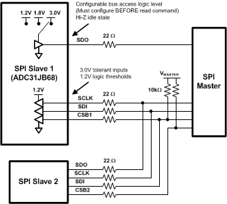
Figure 76 demonstrates a typical circuit to interface the ADC31JB68 device to a SPI master using a shared SPI bus. The 4-wire interface (SCLK, SDI, SDO, CSb) is compatible with 1.2-, 1.8-, or 3.0-V logic. The input pins (SCLK, SDI, CSb) use thick-oxide devices to tolerate 3.0-V logic although the input threshold levels are relative to 1.2-V logic. A low-capacitance protection diode may also be added with the anode connected to the SDO output and the cathode connected to the desired voltage supply to prevent an accidental pre-configured read command from causing damage.
 Figure 76. Typical SPI Application