SBAS671C July 2014 – March 2016 ADC3241 , ADC3242 , ADC3243 , ADC3244
PRODUCTION DATA.
- 1 Features
- 2 Applications
- 3 Description
- 4 Revision History
- 5 Device Comparison Table
- 6 Pin Configuration and Functions
-
7 Specifications
- 7.1 Absolute Maximum Ratings
- 7.2 ESD Ratings
- 7.3 Recommended Operating Conditions
- 7.4 Thermal Information
- 7.5 Electrical Characteristics: ADC3241, ADC3242
- 7.6 Electrical Characteristics: ADC3243, ADC3244
- 7.7 Electrical Characteristics: General
- 7.8 AC Performance: ADC3241
- 7.9 AC Performance: ADC3242
- 7.10 AC Performance: ADC3243
- 7.11 AC Performance: ADC3244
- 7.12 Digital Characteristics
- 7.13 Timing Requirements: General
- 7.14 Timing Requirements: LVDS Output
- 7.15 Typical Characteristics: ADC3241
- 7.16 Typical Characteristics: ADC3242
- 7.17 Typical Characteristics: ADC3243
- 7.18 Typical Characteristics: ADC3244
- 7.19 Typical Characteristics: Common
- 7.20 Typical Characteristics: Contour
- 8 Parameter Measurement Information
-
9 Detailed Description
- 9.1 Overview
- 9.2 Functional Block Diagram
- 9.3 Feature Description
- 9.4 Device Functional Modes
- 9.5 Programming
- 9.6
Register Maps
- 9.6.1 Summary of Special Mode Registers
- 9.6.2
Serial Register Description
- 9.6.2.1 Register 01h
- 9.6.2.2 Register 03h
- 9.6.2.3 Register 04h
- 9.6.2.4 Register 05h
- 9.6.2.5 Register 06h
- 9.6.2.6 Register 07h
- 9.6.2.7 Register 09h
- 9.6.2.8 Register 0Ah
- 9.6.2.9 Register 0Bh
- 9.6.2.10 Register 0Eh
- 9.6.2.11 Register 0Fh
- 9.6.2.12 Register 13h (address = 13h)
- 9.6.2.13 Register 15h
- 9.6.2.14 Register 25h
- 9.6.2.15 Register 27h
- 9.6.2.16 Register 41Dh
- 9.6.2.17 Register 422h
- 9.6.2.18 Register 434h
- 9.6.2.19 Register 439h
- 9.6.2.20 Register 51Dh
- 9.6.2.21 Register 522h
- 9.6.2.22 Register 534h
- 9.6.2.23 Register 539h
- 9.6.2.24 Register 608h
- 9.6.2.25 Register 70Ah
- 10Applications and Implementation
- 11Power-Supply Recommendations
- 12Layout
- 13Device and Documentation Support
- 14Mechanical, Packaging, and Orderable Information
Package Options
Mechanical Data (Package|Pins)
- RGZ|48
Thermal pad, mechanical data (Package|Pins)
- RGZ|48
Orderable Information
12 Layout
12.1 Layout Guidelines
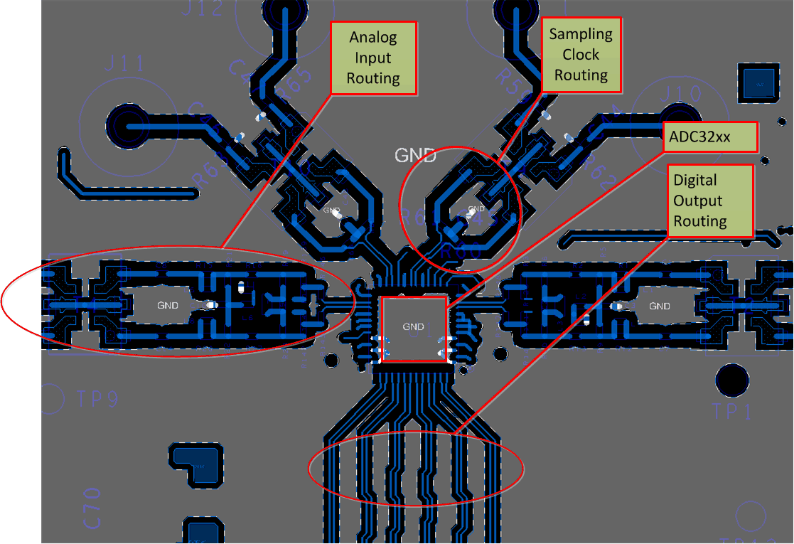
The ADC324x EVM layout can be used as a reference layout to obtain the best performance. A layout diagram of the EVM top layer is provided in Figure 184. Some important points to remember during laying out the board are:
- Analog inputs are located on opposite sides of the device pin out to ensure minimum crosstalk on the package level. To minimize crosstalk onboard, the analog inputs must exit the pin out in opposite directions, as shown in the reference layout of Figure 184 as much as possible.
- In the device pin out, the sampling clock is located on a side perpendicular to the analog inputs in order to minimize coupling between them. This configuration is also maintained on the reference layout of Figure 184 as much as possible.
- Keep digital outputs away from the analog inputs. When these digital outputs exit the pin out, do not keep the digital output traces parallel to the analog input traces because this configuration can result in coupling from digital outputs to analog inputs and degrade performance. All digital output traces to the receiver [such as a field-programmable gate array (FPGA) or an application-specific integrated circuit (ASIC)] must be matched in length to avoid skew among outputs.
- At each power-supply pin (AVDD and DVDD), keep a 0.1-µF decoupling capacitor close to the device. A separate decoupling capacitor group consisting of a parallel combination of 10-µF, 1-µF, and 0.1-µF capacitors can be kept close to the supply source.
12.2 Layout Example
 Figure 184. Typical Layout of the ADC324x Board