SBAS500B june 2022 – august 2023 ADC32RF54 , ADC32RF55
PRODUCTION DATA
- 1
- 1 Features
- 2 Applications
- 3 Description
- 4 Revision History
- 5 Pin Configuration and Functions
-
6 Specifications
- 6.1 Absolute Maximum Ratings
- 6.2 ESD Ratings
- 6.3 Recommended Operating Conditions
- 6.4 Thermal Information
- 6.5 Electrical Characteristics - Power Consumption
- 6.6 Electrical Characteristics - DC Specifications
- 6.7 Electrical Characteristics - ADC32RF54 AC Specifications (Dither DISABLED)
- 6.8 Electrical Characteristics - ADC32RF54 AC Specifications (Dither ENABLED)
- 6.9 Electrical Characteristics - ADC32RF55 AC Specifications (Dither DISABLED)
- 6.10 Electrical Characteristics - ADC32RF55 AC Specifications (Dither ENABLED)
- 6.11 Timing Requirements
- 6.12 Typical Characteristics - ADC32RF54
- 6.13 Typical Characteristics - ADC32RF55
-
7 Detailed Description
- 7.1 Overview
- 7.2 Functional Block Diagram
- 7.3
Feature Description
- 7.3.1 Analog Inputs
- 7.3.2 Sampling Clock Input
- 7.3.3 SYSREF
- 7.3.4 ADC Foreground Calibration
- 7.3.5 Decimation Filter
- 7.3.6
JESD204B Interface
- 7.3.6.1 JESD204B Initial Lane Alignment (ILA)
- 7.3.6.2 JESD204B Frame Assembly
- 7.3.6.3 JESD204B Frame Assembly in Bypass Mode
- 7.3.6.4 JESD204B Frame Assembly with Complex Decimation - Single Band
- 7.3.6.5 JESD204B Frame Assembly with Real Decimation - Single Band
- 7.3.6.6 JESD204B Frame Assembly with Complex Decimation - Dual Band
- 7.3.6.7 JESD204B Frame Assembly with Complex Decimation - Quad Band
- 7.3.7 SERDES Output MUX
- 7.3.8 Test Pattern
- 7.4 Device Functional Modes
- 7.5 Programming
- 7.6 Register Maps
-
8 Application and Implementation
- 8.1 Application Information
- 8.2 Typical Applications
- 8.3
Initialization Set Up
- 8.3.1
Initial Device Configuration After Power-Up
- 8.3.1.1 STEP 1: RESET
- 8.3.1.2 STEP 2: Device Configuration
- 8.3.1.3 STEP 3: JESD Interface Configuration (1)
- 8.3.1.4 STEP 4: SYSREF Synchronization
- 8.3.1.5 STEP 5: JESD Interface Configuration (2)
- 8.3.1.6 STEP 6: Analog Trim Settings
- 8.3.1.7 STEP 7: Calibration Configuration
- 8.3.1.8 STEP 8: SYSREF Synchronization
- 8.3.1.9 STEP 9: Run Power up Calibration
- 8.3.1.10 STEP 10: JESD Interface Synchronization
- 8.3.1
Initial Device Configuration After Power-Up
- 8.4 Power Supply Recommendations
- 8.5 Layout
- 9 Device and Documentation Support
- 10Mechanical, Packaging, and Orderable Information
Package Options
Mechanical Data (Package|Pins)
- RTD|64
Thermal pad, mechanical data (Package|Pins)
- RTD|64
Orderable Information
7.3.2 Sampling Clock Input
The internal sampling clock path was designed for lowest residual phase noise contribution. The sampling clock circuitry requires a dedicated low noise power supply for best performance. The internal residual clock phase noise is also sensitive to clock amplitude. For best performance, the clock amplitude should be larger than 1 VPP. The phase noise ideally improves by 3 dB per 2x averaging, however at higher input frequencies the clock path contribution reduces the improvement.
(FS = 3 Gsps, VIN = 1 VPP)
| Frequency Offset (MHz) | Amplitude (dBc/Hz) |
|---|---|
| 0.001 | -117 |
| 0.01 | -127 |
| 0.1 | -137 |
| 1 | -147 |
| 10 | -154 |
| 250 | -160 |
The clock input and ADC sampling circuitry also have an amplitude noise component which modulates on to the sampled input signal. Unlike phase noise, the amplitude noise does not scale with input frequency, it is only affected by the sampling reset switch as shown in Figure 7-10 and Figure 7-11. This noise component can dominate the close in noise performance at lower input frequencies.
 Figure 7-10 Amplitude Noise vs Input Frequency
 Figure 7-11 Amplitude and Phase noise at 10 kHz offset vs Input Frequency
The internal aperture jitter is also dependent on the amplitude of the external clock input signal. Figure 7-12 and Figure 7-13 show the expected SNR performance with dither on/off across clock amplitude (FS = 2.6 GSPS).
 Figure 7-12 SNR vs Clock Amplitude
(Dither OFF)
 Figure 7-13 SNR vs Clock Amplitude
(Dither ON)
Figure 7-13 SNR vs Clock Amplitude
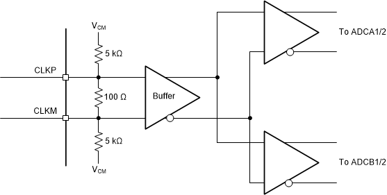
(Dither ON)The sampling clock input is internally terminated to 100 Ω differentially and provides a return loss better than 10 dB at 3 GHz (see Figure 7-14). The clock input consists of a single clock input buffer followed by a dedicated clock buffer for ADCA1/2 as well as ADCB1/2. When averaging multiple ADCs, there are some close in clock buffer noise which is correlated; and thus, does not improve with averaging.
 Figure 7-14 Internal Clock Input
Routing