SBAS500B june 2022 – august 2023 ADC32RF54 , ADC32RF55
PRODUCTION DATA
- 1
- 1 Features
- 2 Applications
- 3 Description
- 4 Revision History
- 5 Pin Configuration and Functions
-
6 Specifications
- 6.1 Absolute Maximum Ratings
- 6.2 ESD Ratings
- 6.3 Recommended Operating Conditions
- 6.4 Thermal Information
- 6.5 Electrical Characteristics - Power Consumption
- 6.6 Electrical Characteristics - DC Specifications
- 6.7 Electrical Characteristics - ADC32RF54 AC Specifications (Dither DISABLED)
- 6.8 Electrical Characteristics - ADC32RF54 AC Specifications (Dither ENABLED)
- 6.9 Electrical Characteristics - ADC32RF55 AC Specifications (Dither DISABLED)
- 6.10 Electrical Characteristics - ADC32RF55 AC Specifications (Dither ENABLED)
- 6.11 Timing Requirements
- 6.12 Typical Characteristics - ADC32RF54
- 6.13 Typical Characteristics - ADC32RF55
-
7 Detailed Description
- 7.1 Overview
- 7.2 Functional Block Diagram
- 7.3
Feature Description
- 7.3.1 Analog Inputs
- 7.3.2 Sampling Clock Input
- 7.3.3 SYSREF
- 7.3.4 ADC Foreground Calibration
- 7.3.5 Decimation Filter
- 7.3.6
JESD204B Interface
- 7.3.6.1 JESD204B Initial Lane Alignment (ILA)
- 7.3.6.2 JESD204B Frame Assembly
- 7.3.6.3 JESD204B Frame Assembly in Bypass Mode
- 7.3.6.4 JESD204B Frame Assembly with Complex Decimation - Single Band
- 7.3.6.5 JESD204B Frame Assembly with Real Decimation - Single Band
- 7.3.6.6 JESD204B Frame Assembly with Complex Decimation - Dual Band
- 7.3.6.7 JESD204B Frame Assembly with Complex Decimation - Quad Band
- 7.3.7 SERDES Output MUX
- 7.3.8 Test Pattern
- 7.4 Device Functional Modes
- 7.5 Programming
- 7.6 Register Maps
-
8 Application and Implementation
- 8.1 Application Information
- 8.2 Typical Applications
- 8.3
Initialization Set Up
- 8.3.1
Initial Device Configuration After Power-Up
- 8.3.1.1 STEP 1: RESET
- 8.3.1.2 STEP 2: Device Configuration
- 8.3.1.3 STEP 3: JESD Interface Configuration (1)
- 8.3.1.4 STEP 4: SYSREF Synchronization
- 8.3.1.5 STEP 5: JESD Interface Configuration (2)
- 8.3.1.6 STEP 6: Analog Trim Settings
- 8.3.1.7 STEP 7: Calibration Configuration
- 8.3.1.8 STEP 8: SYSREF Synchronization
- 8.3.1.9 STEP 9: Run Power up Calibration
- 8.3.1.10 STEP 10: JESD Interface Synchronization
- 8.3.1
Initial Device Configuration After Power-Up
- 8.4 Power Supply Recommendations
- 8.5 Layout
- 9 Device and Documentation Support
- 10Mechanical, Packaging, and Orderable Information
Package Options
Mechanical Data (Package|Pins)
- RTD|64
Thermal pad, mechanical data (Package|Pins)
- RTD|64
Orderable Information
3 Description
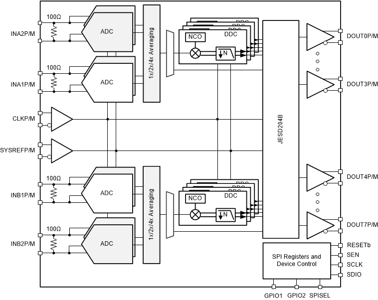
The ADC32RF5x is a single core 14-bit, 2.6 GSPS to 3 GSPS, dual channel analog to digital converters (ADC) that supports RF sampling with input frequencies up to 3 GHz. The design maximizes signal-to-noise ratio (SNR) and delivers a noise spectral density of -155 dBFS/Hz. Using additional internal ADCs along with on-chip signal averaging, the noise density improves to -161 dBFS/Hz.
Each ADC channel can be connected to a quad-band digital down-converter (DDC) using a 48-bit NCO which supports phase coherent frequency hopping. Using the GPIO pins for NCO frequency control, frequency hopping can be achieved in less than 1 µs.
The ADC32RF54 and ADC32RF55 supports the JESD204B serial data interface with subclass 1 deterministic latency using data rates up to 13 Gbps.
The power efficient ADC architecture consumes 2.1 W/ch at 3 Gsps and provides power scaling with lower sampling rates.
| PART NUMBER | SAMPLING RATE |
|---|---|
| ADC32RF55 | 3.0 GSPS |
| ADC32RF54 | 2.6 GSPS |
 Block Diagram