SBAS673A July 2014 – October 2015 ADC3421 , ADC3422 , ADC3423 , ADC3424
PRODUCTION DATA.
- 1 Features
- 2 Applications
- 3 Description
- 4 Revision History
- 5 Device Comparison Table
- 6 Pin Configuration and Functions
-
7 Specifications
- 7.1 Absolute Maximum Ratings
- 7.2 ESD Ratings
- 7.3 Recommended Operating Conditions
- 7.4 Thermal Information
- 7.5 Electrical Characteristics: General
- 7.6 Electrical Characteristics: ADC3421, ADC3422
- 7.7 Electrical Characteristics: ADC3423, ADC3424
- 7.8 AC Performance: ADC3421
- 7.9 AC Performance: ADC3422
- 7.10 AC Performance: ADC3423
- 7.11 AC Performance: ADC3424
- 7.12 Digital Characteristics
- 7.13 Timing Requirements: General
- 7.14 Timing Requirements: LVDS Output
- 7.15 Typical Characteristics: ADC3421
- 7.16 Typical Characteristics: ADC3422
- 7.17 Typical Characteristics: ADC3423
- 7.18 Typical Characteristics: ADC3424
- 7.19 Typical Characteristics: Common
- 7.20 Typical Characteristics: Contour
- 8 Parameter Measurement Information
-
9 Detailed Description
- 9.1 Overview
- 9.2 Functional Block Diagram
- 9.3 Feature Description
- 9.4 Device Functional Modes
- 9.5 Programming
- 9.6
Register Maps
- 9.6.1
Serial Register Description
- 9.6.1.1 Register 13h (address = 13h)
- 9.6.1.2 Register 11Dh (address = 11Dh)
- 9.6.1.3 Register 21Dh (address = 21Dh)
- 9.6.1.4 Register 308h (address = 308h)
- 9.6.1.5 Register 41Dh (address = 41Dh)
- 9.6.1.6 Register 51Dh (address = 51Dh)
- 9.6.1.7 Register 608h (address = 608h)
- 9.6.1.8 Register 70Ah (address = 70Ah)
- 9.6.1
Serial Register Description
- 10Applications and Implementation
- 11Power Supply Recommendations
- 12Layout
- 13Device and Documentation Support
- 14Mechanical, Packaging, and Orderable Information
Package Options
Mechanical Data (Package|Pins)
- RTQ|56
Thermal pad, mechanical data (Package|Pins)
- RTQ|56
Orderable Information
8 Parameter Measurement Information
8.1 Timing Diagrams

1. With an external 100-Ω termination.
Figure 129. Serial LVDS Output Voltage Levels
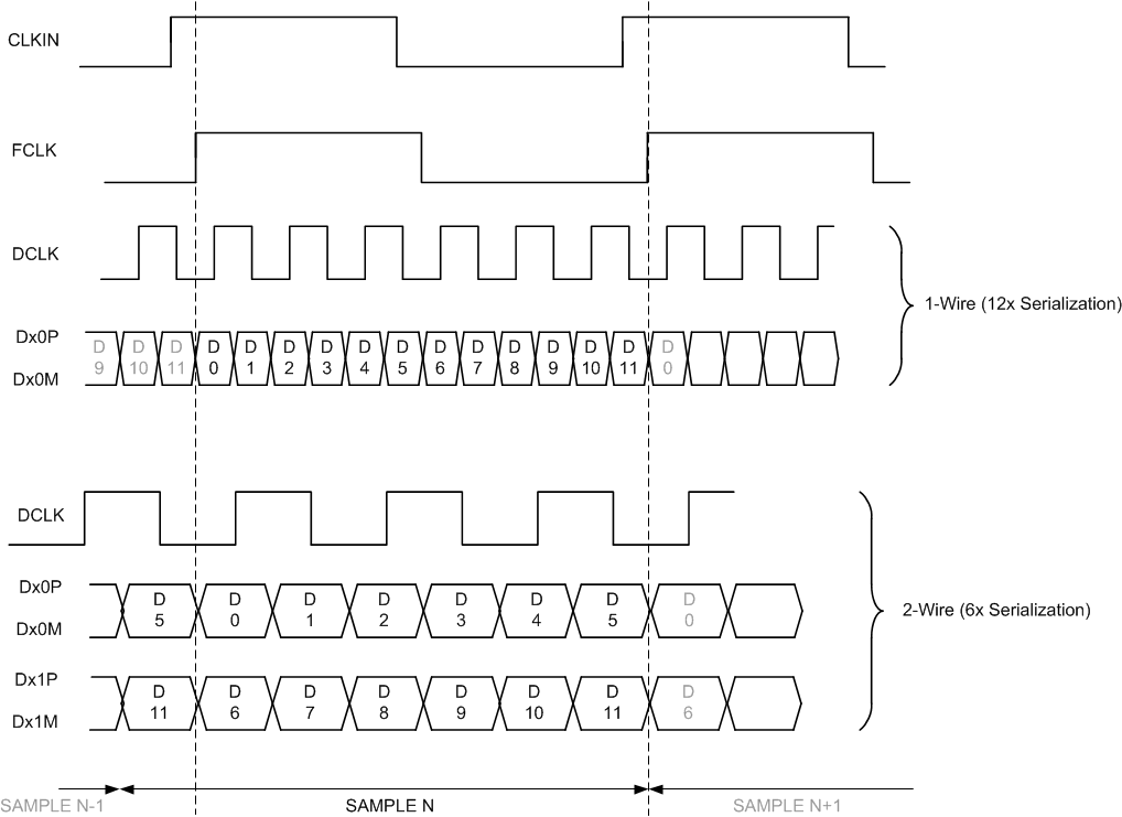
 Figure 130. Output Timing Diagram
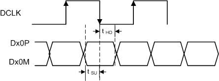
 Figure 131. Setup and Hold Time