SBAS887 August   2022 ADC3564

PRODUCTION DATA  

  1. Features
  2. Applications
  3. Description
  4. Revision History
  5. Pin Configuration and Functions
  6. Specifications
    1. 6.1 Absolute Maximum Ratings
    2. 6.2 ESD Ratings
    3. 6.3 Recommended Operating Conditions
    4. 6.4 Thermal Information
    5. 6.5 Electrical Characteristics - Power Consumption
    6. 6.6 Electrical Characteristics - DC Specifications
    7. 6.7 Electrical Characteristics - AC Specifications
    8. 6.8 Timing Requirements
    9. 6.9 Typical Characteristics
  7. Parameter Measurement Information
  8. Detailed Description
    1. 8.1 Overview
    2. 8.2 Functional Block Diagram
    3. 8.3 Feature Description
      1. 8.3.1 Analog Input
        1. 8.3.1.1 Analog Input Bandwidth
        2. 8.3.1.2 Analog Front End Design
          1. 8.3.1.2.1 Sampling Glitch Filter Design
          2. 8.3.1.2.2 Analog Input Termination and DC Bias
            1. 8.3.1.2.2.1 AC-Coupling
            2. 8.3.1.2.2.2 DC-Coupling
      2. 8.3.2 Clock Input
        1. 8.3.2.1 Single Ended vs Differential Clock Input
      3. 8.3.3 Voltage Reference
        1. 8.3.3.1 Internal voltage reference
        2. 8.3.3.2 External voltage reference (VREF)
        3. 8.3.3.3 External voltage reference with internal buffer (REFBUF)
      4. 8.3.4 Digital Down Converter
        1. 8.3.4.1 DDC MUX for Dual Band Decimation
        2. 8.3.4.2 Digital Filter Operation
        3. 8.3.4.3 FS/4 Mixing with Real Output
        4. 8.3.4.4 Numerically Controlled Oscillator (NCO) and Digital Mixer
        5. 8.3.4.5 Decimation Filter
        6. 8.3.4.6 SYNC
        7. 8.3.4.7 Output Formatting with Decimation
      5. 8.3.5 Digital Interface
        1. 8.3.5.1 Output Formatter
        2. 8.3.5.2 Output Bit Mapper
        3. 8.3.5.3 Output Interface/Mode Configuration
          1. 8.3.5.3.1 Configuration Example
        4. 8.3.5.4 Output Data Format
      6. 8.3.6 Test Pattern
    4. 8.4 Device Functional Modes
      1. 8.4.1 Normal operation
      2. 8.4.2 Power Down Options
    5. 8.5 Programming
      1. 8.5.1 Configuration using PINs only
      2. 8.5.2 Configuration using the SPI interface
        1. 8.5.2.1 Register Write
        2. 8.5.2.2 Register Read
    6. 8.6 Register Maps
      1. 8.6.1 Detailed Register Description
  9. Application Information Disclaimer
    1. 9.1 Typical Application
      1. 9.1.1 Design Requirements
      2. 9.1.2 Detailed Design Procedure
        1. 9.1.2.1 Input Signal Path
        2. 9.1.2.2 Sampling Clock
        3. 9.1.2.3 Voltage Reference
      3. 9.1.3 Application Curves
    2. 9.2 Initialization Set Up
      1. 9.2.1 Register Initialization During Operation
    3. 9.3 Power Supply Recommendations
    4. 9.4 Layout
      1. 9.4.1 Layout Guidelines
      2. 9.4.2 Layout Example
  10. 10Device and Documentation Support
    1. 10.1 Device Support
    2. 10.2 Documentation Support
      1. 10.2.1 Related Documentation
    3. 10.3 Receiving Notification of Documentation Updates
    4. 10.4 Support Resources
    5. 10.5 Trademarks
    6. 10.6 Electrostatic Discharge Caution
    7. 10.7 Glossary
  11. 11Mechanical, Packaging, and Orderable Information

Package Options

Mechanical Data (Package|Pins)
Thermal pad, mechanical data (Package|Pins)
Orderable Information

Description

The ADC3564 device is a low-noise, ultra-low power, 14-bit, 125-MSPS, high-speed ADC. Designed for low power consumption, the device delivers a noise spectral density of –156 dBFS/Hz combined with excellent linearity and dynamic range. The ADC3564 offers IF sampling support which makes the device suited for a wide range of applications. High-speed control loops benefit from the short latency of as little as one clock cycle. The ADC consumes only 137 mW at 125 MSPS, and the power consumption scales well with lower sampling rates.

The ADC3564 uses serial LVDS (SLVDS) interface to output the data which minimizes the number of digital interconnects. The device supports two-lane, one-lane and half-lane options. The device is a pin-to-pin compatible family with different speed grades and comes in a 40-pin VQFN package. The device supports the extended industrial temperature range from –40 to +105⁰C.

Package Information
PART NUMBERPACKAGE(1)BODY SIZE (NOM)
ADC3564WQFN (40)5.00 × 5.00 mm
For all available packages, see the orderable addendum at the end of the data sheet.
Table 3-1 Device Comparison
PART NUMBERRESOLUTIONSAMPLING RATE
ADC356116 BIT10 MSPS
ADC356216 BIT25 MSPS
ADC356316 BIT65 MSPS
ADC356414 BIT125 MSPS
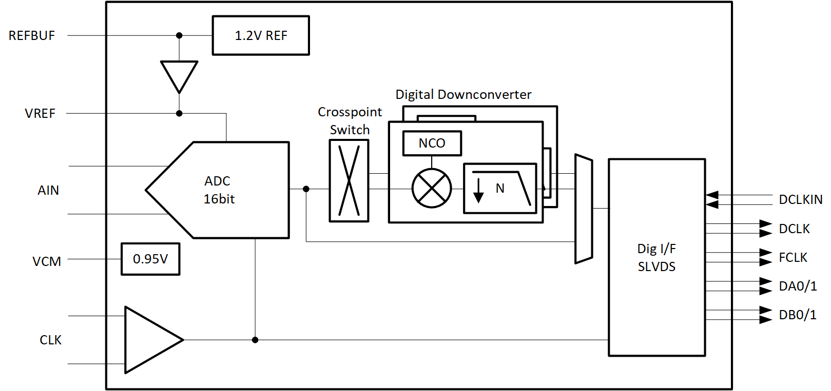
GUID-20200714-CA0I-2RL0-PH0G-K5XX4FFD7KGD-low.gif Simplified Block Diagram