SBASA01B September 2020 – March 2022 ADC3660
PRODUCTION DATA
- 1 Features
- 2 Applications
- 3 Description
- 4 Revision History
- 5 Pin Configuration and Functions
-
6 Specifications
- 6.1 Absolute Maximum Ratings
- 6.2 ESD Ratings
- 6.3 Recommended Operating Conditions
- 6.4 Thermal Information
- 6.5 Electrical Characteristics - Power Consumption
- 6.6 Electrical Characteristics - DC Specifications
- 6.7 Electrical Characteristics - AC Specifications
- 6.8 Timing Requirements
- 6.9 Typical Characteristics
- 7 Parameter Measurement Information
- 8 Detailed Description
- 9 Application and Implementation
- 10Power Supply Recommendations
- 11Layout
- 12Device and Documentation Support
- 13Mechanical, Packaging, and Orderable Information
Package Options
Mechanical Data (Package|Pins)
- RSB|40
Thermal pad, mechanical data (Package|Pins)
- RSB|40
Orderable Information
8.3.4.4 Decimation Filter
The ADC3660 supports complex decimation by 2, 4, 8, 16 and 32 with a pass-band bandwidth of ~ 80% and a stopband rejection of at least 85dB. Table 8-3 gives an overview of the pass-band bandwidth of the different decimation settings with respect to ADC sampling rate FS. Note that the maximum output rate limits can't be exceeded and the ADC sampling rate may need to adjusted. In real decimation mode the output bandwidth is half of the complex bandwidth.
| REAL/COMPLEX DECIMATION | DECIMATION SETTING N | OUTPUT RATE | OUTPUT BANDWIDTH | OUTPUT RATE (FS = 65 MSPS) | OUTPUT BANDWIDTH (FS = 65 MSPS) |
|---|---|---|---|---|---|
| Complex | 2 | FS / 2 complex | 0.8 × FS / 2 | 32.5 MSPS complex | 26 MHz |
| 4 | FS / 4 complex | 0.8 × FS / 4 | 16.25 MSPS complex | 13 MHz | |
| 8 | FS / 8 complex | 0.8 × FS / 8 | 8.125 MSPS complex | 6.5 MHz | |
| 16 | FS / 16 complex | 0.8 × FS / 16 | 4.0625 MSPS complex | 3.25 MHz | |
| 32 | FS / 32 complex | 0.8 × FS / 32 | 2.03125 MSPS complex | 1.625 MHz | |
| Real | 2 | FS / 2 real | 0.4 × FS / 2 | 32.5 MSPS | 13 MHz |
| 4 | FS / 4 real | 0.4 × FS / 4 | 16.25 MSPS | 6.5 MHz | |
| 8 | FS / 8 real | 0.4 × FS / 8 | 8.125 MSPS | 3.25 MHz | |
| 16 | FS / 16 real | 0.4 × FS / 16 | 4.0625 MSPS | 1.625 MHz | |
| 32 | FS / 32 real | 0.4 × FS / 32 | 2.03125 MSPS | 0.8125 MHz |
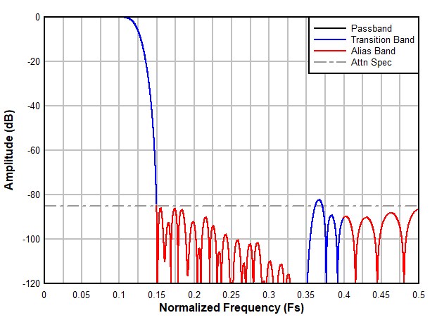
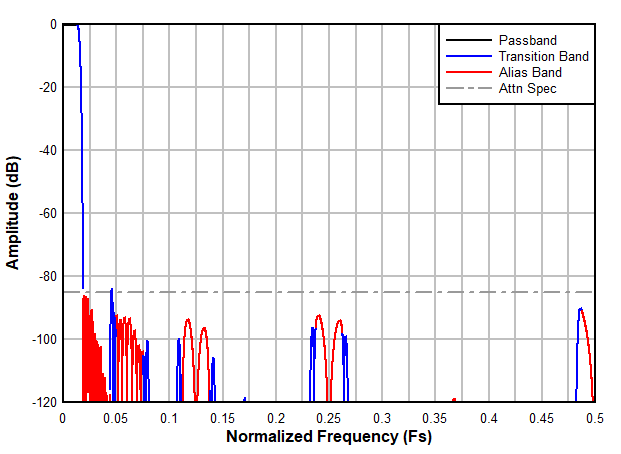
The decimation filter responses normalized tot he ADC sampling clock frequency FS are illustrated in Figure 8-23 to Figure 8-32. They are interpreted as follows:
Each figure contains the filter pass-band, transition band(s) and alias or stop-band(s) as shown in Figure 8-22. The x-axis shows the offset frequency (after the NCO frequency shift) normalized to the ADC sampling rate FS.
For example, in the divide-by-4 complex setup, the output data rate is FS / 4 complex with a Nyquist zone of FS / 8 or 0.125 × FS. The transition band (colored in blue) is centered around 0.125 × FS and the alias transition band is centered at 0.375 × FS. The stop-bands (colored in red), which alias on top of the pass-band, are centered at 0.25 × FS and 0.5 × FS. The stop-band attenuation is greater than 85 dB.
 Figure 8-22 Interpretation of the Decimation Filter Plots
 Figure 8-23 Decimation by 2 complex frequency response
 Figure 8-25 Decimation by 4complex frequency response
 Figure 8-27 Decimation by 8 complex frequency response
 Figure 8-29 Decimation by 16 complex frequency response
 Figure 8-31 Decimation by 32 complex frequency response
 Figure 8-24 Decimation by 2 complex passband ripple response
 Figure 8-26 Decimation by 4 complex passband ripple response
 Figure 8-28 Decimation by 8 complex passband ripple response
 Figure 8-30 Decimation by 16 complex passband ripple response
 Figure 8-32 Decimation by 32 complex passband ripple response