SBAS872B December   2020  – October 2022 ADC3681 , ADC3682 , ADC3683

PRODUCTION DATA  

  1. Features
  2. Applications
  3. Description
  4. Revision History
  5. Pin Configuration and Functions
  6. Specifications
    1. 6.1  Absolute Maximum Ratings
    2. 6.2  ESD Ratings
    3. 6.3  Recommended Operating Conditions
    4. 6.4  Thermal Information
    5. 6.5  Electrical Characteristics - Power Consumption
    6. 6.6  Electrical Characteristics - DC Specifications
    7. 6.7  Electrical Characteristics - AC Specifications
    8. 6.8  Timing Requirements
    9. 6.9  Typical Characteristics - ADC3681
    10. 6.10 Typical Characteristics - ADC3682
    11. 6.11 Typical Characteristics - ADC3683
  7. Parameter Measurement Information
  8. Detailed Description
    1. 8.1 Overview
    2. 8.2 Functional Block Diagram
    3. 8.3 Feature Description
      1. 8.3.1 Analog Input
        1. 8.3.1.1 Analog Input Bandwidth
        2. 8.3.1.2 Analog Front End Design
          1. 8.3.1.2.1 Sampling Glitch Filter Design
          2. 8.3.1.2.2 Analog Input Termination and DC Bias
            1. 8.3.1.2.2.1 AC-Coupling
            2. 8.3.1.2.2.2 DC-Coupling
        3. 8.3.1.3 Auto-Zero Feature
      2. 8.3.2 Clock Input
        1. 8.3.2.1 Single Ended vs Differential Clock Input
        2. 8.3.2.2 Signal Acquisition Time Adjust
      3. 8.3.3 Voltage Reference
        1. 8.3.3.1 Internal voltage reference
        2. 8.3.3.2 External voltage reference (VREF)
        3. 8.3.3.3 External voltage reference with internal buffer (REFBUF)
      4. 8.3.4 Digital Down Converter
        1. 8.3.4.1 DDC MUX
        2. 8.3.4.2 Digital Filter Operation
        3. 8.3.4.3 FS/4 Mixing with Real Output
        4. 8.3.4.4 Numerically Controlled Oscillator (NCO) and Digital Mixer
        5. 8.3.4.5 Decimation Filter
        6. 8.3.4.6 SYNC
        7. 8.3.4.7 Output Formatting with Decimation
      5. 8.3.5 Digital Interface
        1. 8.3.5.1 Output Formatter
        2. 8.3.5.2 Output Scrambler
        3. 8.3.5.3 Output Bit Mapper
        4. 8.3.5.4 Output Interface/Mode Configuration
          1. 8.3.5.4.1 Configuration Example
        5. 8.3.5.5 Output Data Format
      6. 8.3.6 Test Pattern
    4. 8.4 Device Functional Modes
      1. 8.4.1 Normal Operation
      2. 8.4.2 Power Down Options
      3. 8.4.3 Digital Channel Averaging
    5. 8.5 Programming
      1. 8.5.1 Configuration using PINs only
      2. 8.5.2 Configuration using the SPI interface
        1. 8.5.2.1 Register Write
        2. 8.5.2.2 Register Read
    6. 8.6 Register Map
      1. 8.6.1 Detailed Register Description
  9. Application Information Disclaimer
    1. 9.1 Typical Application
      1. 9.1.1 Design Requirements
      2. 9.1.2 Detailed Design Procedure
        1. 9.1.2.1 Input Signal Path
        2. 9.1.2.2 Sampling Clock
        3. 9.1.2.3 Voltage Reference
      3. 9.1.3 Application Curves
    2. 9.2 Initialization Set Up
      1. 9.2.1 Register Initialization During Operation
    3. 9.3 Power Supply Recommendations
    4. 9.4 Layout
      1. 9.4.1 Layout Guidelines
      2. 9.4.2 Layout Example
  10. 10Device and Documentation Support
    1. 10.1 Receiving Notification of Documentation Updates
    2. 10.2 Support Resources
    3. 10.3 Trademarks
    4. 10.4 Electrostatic Discharge Caution
    5. 10.5 Glossary
  11. 11Mechanical, Packaging, and Orderable Information

Package Options

Mechanical Data (Package|Pins)
Thermal pad, mechanical data (Package|Pins)
Orderable Information

Analog Input

The analog inputs of ADC368x are intended to be driven differentially. Both AC coupling and DC coupling of the analog inputs is supported. The analog inputs are designed for an input common mode voltage of 0.95 V which must be provided externally on each input pin. DC-coupled input signals must have a common mode voltage that meets the device input common mode voltage range.

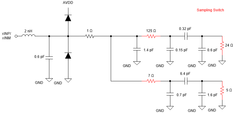
The equivalent input network diagram is shown in Figure 8-1. All four sampling switches, on-resistance shown in red are in same position (open or closed) simultaneously.
GUID-8184E1FE-AF55-452A-8F8E-E2B5001D672A-low.gif Figure 8-1 Equivalent input network