SBAS473E May 2009 – January 2018 ADS1013 , ADS1014 , ADS1015
PRODUCTION DATA.
- 1 Features
- 2 Applications
- 3 Description
- 4 Revision History
- 5 Device Comparison Table
- 6 Pin Configuration and Functions
- 7 Specifications
-
8 Detailed Description
- 8.1 Overview
- 8.2 Functional Block Diagrams
- 8.3 Feature Description
- 8.4 Device Functional Modes
- 8.5 Programming
- 8.6 Register Map
-
9 Application and Implementation
- 9.1 Application Information
- 9.2
Typical Application
- 9.2.1 Design Requirements
- 9.2.2
Detailed Design Procedure
- 9.2.2.1 Shunt Resistor Considerations
- 9.2.2.2 Operational Amplifier Considerations
- 9.2.2.3 ADC Input Common-Mode Considerations
- 9.2.2.4 Resistor (R1, R2, R3, R4) Considerations
- 9.2.2.5 Noise and Input Impedance Considerations
- 9.2.2.6 First-order RC Filter Considerations
- 9.2.2.7 Circuit Implementation
- 9.2.2.8 Results Summary
- 9.2.3 Application Curves
- 10Power Supply Recommendations
- 11Layout
- 12Device and Documentation Support
- 13Mechanical, Packaging, and Orderable Information
Package Options
Mechanical Data (Package|Pins)
Thermal pad, mechanical data (Package|Pins)
Orderable Information
9.1.5 Analog Input Filtering
Analog input filtering serves two purposes:
- Limits the effect of aliasing during the sampling process
- Reduces external noise from being a part of the measurement
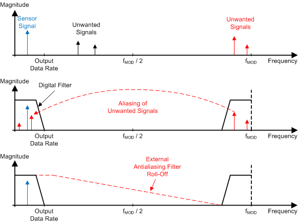
Aliasing occurs when frequency components are present in the input signal that are higher than half the sampling frequency of the ADC (also known as the Nyquist frequency). These frequency components fold back and show up in the actual frequency band of interest below half the sampling frequency. The filter response of the digital filter repeats at multiples of the sampling frequency, also known as the modulator frequency (fMOD), as shown in Figure 26. Signals or noise up to a frequency where the filter response repeats are attenuated to a certain amount by the digital filter depending on the filter architecture. Any frequency components present in the input signal around the modulator frequency, or multiples thereof, are not attenuated and alias back into the band of interest, unless attenuated by an external analog filter.
 Figure 26. Effect of Aliasing
Many sensor signals are inherently band-limited; for example, the output of a thermocouple has a limited rate of change. In this case, the sensor signal does not alias back into the pass-band when using a ΔΣ ADC. However, any noise pick-up along the sensor wiring or the application circuitry can potentially alias into the pass-band. Power line-cycle frequency and harmonics are one common noise source. External noise can also be generated from electromagnetic interference (EMI) or radio frequency interference (RFI) sources, such as nearby motors and cellular phones. Another noise source typically exists on the printed-circuit-board (PCB) itself in the form of clocks and other digital signals. Analog input filtering helps remove unwanted signals from affecting the measurement result.
A first-order resistor-capacitor (RC) filter is (in most cases) sufficient to either totally eliminate aliasing, or to reduce the effect of aliasing to a level within the noise floor of the sensor. Ideally, any signal beyond fMOD / 2 is attenuated to a level below the noise floor of the ADC. The digital filter of the ADS101x attenuate signals to a certain degree. In addition, noise components are usually smaller in magnitude than the actual sensor signal. Therefore, use a first-order RC filter with a cutoff frequency set at the output data rate or 10x higher as a generally good starting point for a system design.