SBAS741B October   2015  – April 2020 ADS1018-Q1

PRODUCTION DATA.  

  1. Features
  2. Applications
  3. Description
    1.     Device Images
      1.      K-Type Thermocouple Measurement Using Integrated Temperature Sensor for Cold-Junction Compensation
  4. Revision History
  5. Device Comparison Table
  6. Pin Configuration and Functions
    1.     Pin Functions
  7. Specifications
    1. 7.1 Absolute Maximum Ratings
    2. 7.2 ESD Ratings
    3. 7.3 Recommended Operating Conditions
    4. 7.4 Thermal Information
    5. 7.5 Electrical Characteristics
    6. 7.6 Timing Requirements: Serial Interface
    7. 7.7 Switching Characteristics: Serial Interface
    8. 7.8 Typical Characteristics
  8. Detailed Description
    1. 8.1 Overview
    2. 8.2 Functional Block Diagram
    3. 8.3 Feature Description
      1. 8.3.1 Multiplexer
      2. 8.3.2 Analog Inputs
      3. 8.3.3 Full-Scale Range (FSR) and LSB Size
      4. 8.3.4 Voltage Reference
      5. 8.3.5 Oscillator
      6. 8.3.6 Temperature Sensor
        1. 8.3.6.1 Converting from Temperature to Digital Codes
        2. 8.3.6.2 Converting from Digital Codes to Temperature
    4. 8.4 Device Functional Modes
      1. 8.4.1 Reset and Power-Up
      2. 8.4.2 Operating Modes
        1. 8.4.2.1 Single-Shot Mode and Power-Down
        2. 8.4.2.2 Continuous-Conversion Mode
      3. 8.4.3 Duty Cycling for Low Power
    5. 8.5 Programming
      1. 8.5.1 Serial Interface
      2. 8.5.2 Chip Select (CS)
      3. 8.5.3 Serial Clock (SCLK)
      4. 8.5.4 Data Input (DIN)
      5. 8.5.5 Data Output and Data Ready (DOUT/DRDY)
      6. 8.5.6 Data Format
      7. 8.5.7 Data Retrieval
        1. 8.5.7.1 32-Bit Data Transmission Cycle
        2. 8.5.7.2 16-Bit Data Transmission Cycle
    6. 8.6 Register Maps
      1. 8.6.1 Conversion Register [reset = 0000h]
        1. Table 4. Conversion Register Field Descriptions
      2. 8.6.2 Config Register [reset = 058Bh]
        1. Table 5. Config Register Field Descriptions
  9. Application and Implementation
    1. 9.1 Application Information
      1. 9.1.1 Serial Interface Connections
      2. 9.1.2 GPIO Ports for Communication
      3. 9.1.3 Analog Input Filtering
      4. 9.1.4 Single-Ended Inputs
      5. 9.1.5 Connecting Multiple Devices
      6. 9.1.6 Pseudo Code Example
    2. 9.2 Typical Application
      1. 9.2.1 Design Requirements
      2. 9.2.2 Detailed Design Procedure
      3. 9.2.3 Application Curves
  10. 10Power Supply Recommendations
    1. 10.1 Power-Supply Sequencing
    2. 10.2 Power-Supply Decoupling
  11. 11Layout
    1. 11.1 Layout Guidelines
    2. 11.2 Layout Example
  12. 12Device and Documentation Support
    1. 12.1 Documentation Support
      1. 12.1.1 Related Documentation
    2. 12.2 Receiving Notification of Documentation Updates
    3. 12.3 Community Resources
    4. 12.4 Trademarks
    5. 12.5 Electrostatic Discharge Caution
    6. 12.6 Glossary
  13. 13Mechanical, Packaging, and Orderable Information

Package Options

Mechanical Data (Package|Pins)
Thermal pad, mechanical data (Package|Pins)
Orderable Information

Single-Ended Inputs

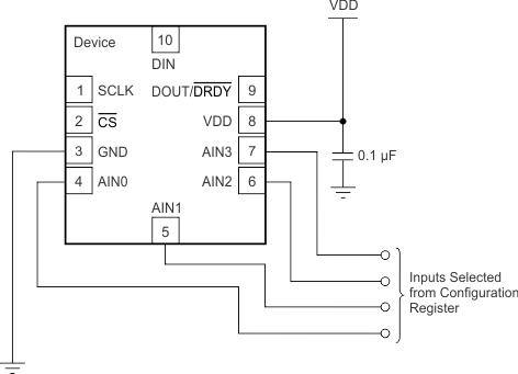
Although the ADS1018-Q1 has two differential inputs, the device can measure four single-ended signals. Figure 20 shows a single-ended connection scheme. The ADS1018-Q1 is configured for single-ended measurement by configuring the mux to measure each channel with respect to ground. Data are then read out of one input based on the selection in the Config register. The single-ended signal can range from 0 V up to positive supply or +FS, whichever is lower. Negative voltages cannot be applied to this circuit because the ADS1018-Q1 can only accept positive voltages with respect to ground. The ADS1018-Q1 does not lose linearity within the input range.

The ADS1018-Q1 offers a differential input voltage range of ±FS. The single-ended circuit shown in Figure 20, however, only uses the positive half of the ADS1018-Q1 FS input voltage range because differentially negative inputs are not produced. Because only half of the FS range is used, one bit of resolution is lost. For optimal noise performance, use differential configurations whenever possible. Differential configurations maximize the dynamic range of the ADC and provide strong attenuation of common-mode noise.
ADS1018-Q1 ai_msr_1end_inputs_bas457.gif

NOTE:

Digital pin connections omitted for clarity.
Figure 20. Measuring Single-Ended Inputs

The ADS1018-Q1 also allows AIN3 to serve as a common point for measurements by adjusting the mux configuration. AIN0, AIN1, and AIN2 can all be measured with respect to AIN3. In this configuration, the ADS1018-Q1 operates with inputs where AIN3 serves as the common point. This ability improves the usable range over the single-ended configuration because negative differential voltages are allowed when GND < V(AIN3) < VDD; however, common-mode noise attenuation is not offered.