SBAS444E May   2009  – December 2024 ADS1113 , ADS1114 , ADS1115

PRODUCTION DATA  

  1.   1
  2. Features
  3. Applications
  4. Description
  5.   Device Comparison Table
  6. Pin Configuration and Functions
  7. Specifications
    1. 5.1 Absolute Maximum Ratings
    2. 5.2 ESD Ratings
    3. 5.3 Recommended Operating Conditions
    4. 5.4 Thermal Information
    5. 5.5 Electrical Characteristics
    6. 5.6 Timing Requirements: I2C
    7. 5.7 Typical Characteristics
  8. Parameter Measurement Information
    1. 6.1 Noise Performance
  9. Detailed Description
    1. 7.1 Overview
    2. 7.2 Functional Block Diagrams
    3. 7.3 Feature Description
      1. 7.3.1 Multiplexer
      2. 7.3.2 Analog Inputs
      3. 7.3.3 Full-Scale Range (FSR) and LSB Size
      4. 7.3.4 Voltage Reference
      5. 7.3.5 Oscillator
      6. 7.3.6 Output Data Rate and Conversion Time
      7. 7.3.7 Digital Comparator (ADS1114 and ADS1115 Only)
      8. 7.3.8 Conversion Ready Pin (ADS1114 and ADS1115 Only)
      9. 7.3.9 SMbus Alert Response
    4. 7.4 Device Functional Modes
      1. 7.4.1 Reset and Power-Up
      2. 7.4.2 Operating Modes
        1. 7.4.2.1 Single-Shot Mode
        2. 7.4.2.2 Continuous-Conversion Mode
      3. 7.4.3 Duty Cycling For Low Power
    5. 7.5 Programming
      1. 7.5.1 I2C Interface
        1. 7.5.1.1 I2C Address Selection
        2. 7.5.1.2 I2C General Call
        3. 7.5.1.3 I2C Speed Modes
      2. 7.5.2 Target Mode Operations
        1. 7.5.2.1 Receive Mode
        2. 7.5.2.2 Transmit Mode
      3. 7.5.3 Writing To and Reading From the Registers
      4. 7.5.4 Data Format
  10. Registers
    1. 8.1 Register Map
      1. 8.1.1 Address Pointer Register (address = N/A) [reset = N/A]
      2. 8.1.2 Conversion Register (P[1:0] = 00b) [reset = 0000h]
      3. 8.1.3 Config Register (P[1:0] = 01b) [reset = 8583h]
      4. 8.1.4 Lo_thresh (P[1:0] = 10b) [reset = 8000h] and Hi_thresh (P[1:0] = 11b) [reset = 7FFFh] Registers
  11. Application and Implementation
    1. 9.1 Application Information
      1. 9.1.1 Basic Connections
      2. 9.1.2 Single-Ended Inputs
      3. 9.1.3 Input Protection
      4. 9.1.4 Unused Inputs and Outputs
      5. 9.1.5 Analog Input Filtering
      6. 9.1.6 Connecting Multiple Devices
      7. 9.1.7 Quick-Start Guide
    2. 9.2 Typical Application
      1. 9.2.1 Design Requirements
      2. 9.2.2 Detailed Design Procedure
        1. 9.2.2.1 Shunt Resistor Considerations
        2. 9.2.2.2 Operational Amplifier Considerations
        3. 9.2.2.3 ADC Input Common-Mode Considerations
        4. 9.2.2.4 Resistor (R1, R2, R3, R4) Considerations
        5. 9.2.2.5 Noise and Input Impedance Considerations
        6. 9.2.2.6 First-Order RC Filter Considerations
        7. 9.2.2.7 Circuit Implementation
        8. 9.2.2.8 Results Summary
      3. 9.2.3 Application Curves
  12. 10Power Supply Recommendations
    1. 10.1 Power-Supply Sequencing
    2. 10.2 Power-Supply Decoupling
  13. 11Layout
    1. 11.1 Layout Guidelines
    2. 11.2 Layout Example
  14. 12Device and Documentation Support
    1. 12.1 Documentation Support
      1. 12.1.1 Related Documentation
    2. 12.2 Receiving Notification of Documentation Updates
    3. 12.3 Support Resources
    4. 12.4 Trademarks
    5. 12.5 Electrostatic Discharge Caution
    6. 12.6 Glossary
  15. 13Revision History
  16. 14Mechanical, Packaging, and Orderable Information

Package Options

Mechanical Data (Package|Pins)
Thermal pad, mechanical data (Package|Pins)
Orderable Information

Data Format

The ADS111x provide 16 bits of data in binary 2's-complement format. A positive full-scale (+FS) input produces an output code of 7FFFh and a negative full-scale (–FS) input produces an output code of 8000h. The output clips at these codes for signals that exceed full-scale. Table 7-3 summarizes the ideal output codes for different input signals. Figure 7-12 shows code transitions versus input voltage.

Table 7-3 Input Signal Versus Ideal Output Code
INPUT SIGNAL
VIN = (VAINP – VAINN)
IDEAL OUTPUT CODE(1)(1)
≥ +FS (215 – 1)/2157FFFh
+FS/2150001h
00000h
–FS/215FFFFh
≤ –FS8000h
Excludes the effects of noise, INL, offset, and gain errors.
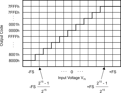
ADS1113 ADS1114 ADS1115 Code Transition DiagramFigure 7-12 Code Transition Diagram
Note: Single-ended signal measurements, where VAINN = 0V and VAINP = 0V to +FS, only use the positive code range from 0000h to 7FFFh. However, because of device offset, the ADS111x can still output negative codes in case VAINP is close to 0V.