SBASAV5 December   2023 ADS1114L , ADS1115L

PRODUCTION DATA  

  1.   1
  2. Features
  3. Applications
  4. Description
  5. Device Comparison Table
  6. Pin Configuration and Functions
  7. Specifications
    1. 6.1 Absolute Maximum Ratings
    2. 6.2 ESD Ratings
    3. 6.3 Recommended Operating Conditions
    4. 6.4 Thermal Information
    5. 6.5 Electrical Characteristics
    6. 6.6 I2C Timing Requirements
    7. 6.7 Timing Diagram
    8. 6.8 Typical Characteristics
  8. Parameter Measurement Information
    1. 7.1 Noise Performance
  9. Detailed Description
    1. 8.1 Overview
    2. 8.2 Functional Block Diagrams
    3. 8.3 Feature Description
      1. 8.3.1 Multiplexer
      2. 8.3.2 Analog Inputs
      3. 8.3.3 Full-Scale Range (FSR) and LSB Size
      4. 8.3.4 Voltage Reference
      5. 8.3.5 Oscillator
      6. 8.3.6 Output Data Rate and Conversion Time
      7. 8.3.7 Digital Comparator
      8. 8.3.8 Conversion-Ready Pin
      9. 8.3.9 SMBus Alert Response
    4. 8.4 Device Functional Modes
      1. 8.4.1 Reset and Power-Up
      2. 8.4.2 Operating Modes
        1. 8.4.2.1 Single-Shot Mode
        2. 8.4.2.2 Continuous-Conversion Mode
    5. 8.5 Programming
      1. 8.5.1 I2C Interface
        1. 8.5.1.1 I2C Address Selection
        2. 8.5.1.2 I2C Interface Speed
          1. 8.5.1.2.1 Serial Clock (SCL) and Serial Data (SDA)
        3. 8.5.1.3 I2C Data Transfer Protocol
        4. 8.5.1.4 Timeout
        5. 8.5.1.5 I2C General-Call (Software Reset)
      2. 8.5.2 Reading and Writing Register Data
        1. 8.5.2.1 Reading Conversion Data or the Configuration Register
        2. 8.5.2.2 Writing the Configuration Register
      3. 8.5.3 Data Format
  10. Register Map
  11. 10Application and Implementation
    1. 10.1 Application Information
      1. 10.1.1 Basic Connections
      2. 10.1.2 Unused Inputs and Outputs
      3. 10.1.3 Single-Ended Inputs
      4. 10.1.4 Input Protection
      5. 10.1.5 Analog Input Filtering
      6. 10.1.6 Connecting Multiple Devices
      7. 10.1.7 Duty Cycling For Low Power
      8. 10.1.8 I2C Communication Sequence Example
    2. 10.2 Typical Application
      1. 10.2.1 Design Requirements
      2. 10.2.2 Detailed Design Procedure
      3. 10.2.3 Application Curve
    3. 10.3 Power Supply Recommendations
      1. 10.3.1 Power-Supply Sequencing
      2. 10.3.2 Power-Supply Decoupling
    4. 10.4 Layout
      1. 10.4.1 Layout Guidelines
      2. 10.4.2 Layout Example
  12. 11Device and Documentation Support
    1. 11.1 Receiving Notification of Documentation Updates
    2. 11.2 Support Resources
    3. 11.3 Trademarks
    4. 11.4 Electrostatic Discharge Caution
    5. 11.5 Glossary
  13. 12Revision History
  14. 13Mechanical, Packaging, and Orderable Information

Package Options

Mechanical Data (Package|Pins)
Thermal pad, mechanical data (Package|Pins)
Orderable Information

Application Curve

The measurement results in Figure 10-10 show that the two supplies can be measured with ±0.5% accuracy over the complete operating ambient temperature range without any offset or gain calibration.
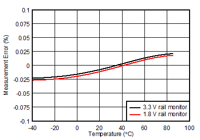
ADS1114L ADS1115L Measurement Error vs TemperatureFigure 10-10 Measurement Error vs Temperature