SBAS563E December 2011 – December 2022 ADS1113-Q1 , ADS1114-Q1 , ADS1115-Q1
PRODUCTION DATA
- 1 Features
- 2 Applications
- 3 Description
- 4 Revision History
- 5 Pin Configuration and Functions
- 6 Specifications
- 7 Parameter Measurement Information
-
8 Detailed Description
- 8.1 Overview
- 8.2 Functional Block Diagrams
- 8.3
Feature Description
- 8.3.1 Multiplexer
- 8.3.2 Analog Inputs
- 8.3.3 Full-Scale Range (FSR) and LSB Size
- 8.3.4 Voltage Reference
- 8.3.5 Oscillator
- 8.3.6 Output Data Rate and Conversion Time
- 8.3.7 Digital Comparator (ADS1114-Q1 and ADS1115-Q1 Only)
- 8.3.8 Conversion Ready Pin (ADS1114-Q1 and ADS1115-Q1 Only)
- 8.3.9 SMbus Alert Response
- 8.4 Device Functional Modes
- 8.5 Programming
- 8.6 Register Map
-
9 Application and Implementation
- 9.1 Application Information
- 9.2
Typical Application
- 9.2.1 Design Requirements
- 9.2.2
Detailed Design Procedure
- 9.2.2.1 Shunt Resistor Considerations
- 9.2.2.2 Operational Amplifier Considerations
- 9.2.2.3 ADC Input Common-Mode Considerations
- 9.2.2.4 Resistor (R1, R2, R3, R4) Considerations
- 9.2.2.5 Noise and Input Impedance Considerations
- 9.2.2.6 First-Order RC Filter Considerations
- 9.2.2.7 Circuit Implementation
- 9.2.2.8 Results Summary
- 9.2.3 Application Curves
- 9.3 Power Supply Recommendations
- 9.4 Layout
- 10Device and Documentation Support
- 11Mechanical, Packaging, and Orderable Information
Package Options
Mechanical Data (Package|Pins)
Thermal pad, mechanical data (Package|Pins)
Orderable Information
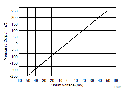
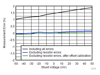
9.2.3 Application Curves
 Figure 9-7 Measured Output vs Shunt Voltage (VSHUNT)
 Figure 9-8 Measurement Error vs Shunt Voltage (VSHUNT)