SBAS740B October   2015  – May 2020 ADS1118-Q1

PRODUCTION DATA.  

  1. Features
  2. Applications
  3. Description
    1.     Device Images
      1.      K-Type Thermocouple Measurement Using Integrated Temperature Sensor for Cold-Junction Compensation
  4. Revision History
  5. Device Comparison Table
  6. Pin Configuration and Functions
    1.     Pin Functions
  7. Specifications
    1. 7.1 Absolute Maximum Ratings
    2. 7.2 ESD Ratings
    3. 7.3 Recommended Operating Conditions
    4. 7.4 Thermal Information
    5. 7.5 Electrical Characteristics
    6. 7.6 Timing Requirements: Serial Interface
    7. 7.7 Switching Characteristics: Serial Interface
    8. 7.8 Typical Characteristics
  8. Parameter Measurement Information
    1. 8.1 Noise Performance
  9. Detailed Description
    1. 9.1 Overview
    2. 9.2 Functional Block Diagram
    3. 9.3 Feature Description
      1. 9.3.1 Multiplexer
      2. 9.3.2 Analog Inputs
      3. 9.3.3 Full-Scale Range (FSR) and LSB Size
      4. 9.3.4 Voltage Reference
      5. 9.3.5 Oscillator
      6. 9.3.6 Temperature Sensor
        1. 9.3.6.1 Converting from Temperature to Digital Codes
        2. 9.3.6.2 Converting from Digital Codes to Temperature
    4. 9.4 Device Functional Modes
      1. 9.4.1 Reset and Power-Up
      2. 9.4.2 Operating Modes
        1. 9.4.2.1 Single-Shot Mode and Power-Down
        2. 9.4.2.2 Continuous-Conversion Mode
      3. 9.4.3 Duty Cycling for Low Power
    5. 9.5 Programming
      1. 9.5.1 Serial Interface
      2. 9.5.2 Chip Select (CS)
      3. 9.5.3 Serial Clock (SCLK)
      4. 9.5.4 Data Input (DIN)
      5. 9.5.5 Data Output and Data Ready (DOUT/DRDY)
      6. 9.5.6 Data Format
      7. 9.5.7 Data Retrieval
        1. 9.5.7.1 32-Bit Data Transmission Cycle
        2. 9.5.7.2 16-Bit Data Transmission Cycle
    6. 9.6 Register Maps
      1. 9.6.1 Conversion Register [reset = 0000h]
        1. Table 6. Conversion Register Field Descriptions
      2. 9.6.2 Config Register [reset = 058Bh]
        1. Table 7. Config Register Field Descriptions
  10. 10Application and Implementation
    1. 10.1 Application Information
      1. 10.1.1 Serial Interface Connections
      2. 10.1.2 GPIO Ports for Communication
      3. 10.1.3 Analog Input Filtering
      4. 10.1.4 Single-Ended Inputs
      5. 10.1.5 Connecting Multiple Devices
      6. 10.1.6 Pseudo Code Example
    2. 10.2 Typical Application
      1. 10.2.1 Design Requirements
      2. 10.2.2 Detailed Design Procedure
      3. 10.2.3 Application Curves
  11. 11Power Supply Recommendations
    1. 11.1 Power-Supply Sequencing
    2. 11.2 Power-Supply Decoupling
  12. 12Layout
    1. 12.1 Layout Guidelines
    2. 12.2 Layout Example
  13. 13Device and Documentation Support
    1. 13.1 Documentation Support
      1. 13.1.1 Related Documentation
    2. 13.2 Receiving Notification of Documentation Updates
    3. 13.3 Support Resources
    4. 13.4 Trademarks
    5. 13.5 Electrostatic Discharge Caution
    6. 13.6 Glossary
  14. 14Mechanical, Packaging, and Orderable Information

Package Options

Mechanical Data (Package|Pins)
Thermal pad, mechanical data (Package|Pins)
Orderable Information

Pin Configuration and Functions

DGS Package
10-Pin VSSOP
Top View
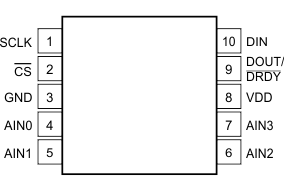
ADS1118-Q1 po_dgs_bas457.gif

Pin Functions

PIN TYPE DESCRIPTION
NO. NAME
1 SCLK Digital input Serial clock input
2 CS Digital input Chip select; active low. Connect to GND if not used.
3 GND Supply Ground
4 AIN0 Analog input Analog input 0. Leave unconnected or tie to VDD if not used.
5 AIN1 Analog input Analog input 1. Leave unconnected or tie to VDD if not used.
6 AIN2 Analog input Analog input 2. Leave unconnected or tie to VDD if not used.
7 AIN3 Analog input Analog input 3. Leave unconnected or tie to VDD if not used.
8 VDD Supply Power supply. Connect a 0.1-µF power supply decoupling capacitor to GND.
9 DOUT/DRDY Digital output Serial data output combined with data ready; active low
10 DIN Digital input Serial data input