SBAS457F October   2010  – September 2019 ADS1118

PRODUCTION DATA.  

  1. Features
  2. Applications
  3. Description
    1.     Device Images
      1.      K-Type Thermocouple Measurement Using Integrated Temperature Sensor for Cold-Junction Compensation
  4. Revision History
  5. Device Comparison Table
  6. Pin Configuration and Functions
    1.     Pin Functions
  7. Specifications
    1. 7.1 Absolute Maximum Ratings
    2. 7.2 ESD Ratings
    3. 7.3 Recommended Operating Conditions
    4. 7.4 Thermal Information
    5. 7.5 Electrical Characteristics
    6. 7.6 Timing Requirements: Serial Interface
    7. 7.7 Switching Characteristics: Serial Interface
    8. 7.8 Typical Characteristics
  8. Parameter Measurement Information
    1. 8.1 Noise Performance
  9. Detailed Description
    1. 9.1 Overview
    2. 9.2 Functional Block Diagram
    3. 9.3 Feature Description
      1. 9.3.1 Multiplexer
      2. 9.3.2 Analog Inputs
      3. 9.3.3 Full-Scale Range (FSR) and LSB Size
      4. 9.3.4 Voltage Reference
      5. 9.3.5 Oscillator
      6. 9.3.6 Temperature Sensor
        1. 9.3.6.1 Converting from Temperature to Digital Codes
        2. 9.3.6.2 Converting from Digital Codes to Temperature
    4. 9.4 Device Functional Modes
      1. 9.4.1 Reset and Power Up
      2. 9.4.2 Operating Modes
        1. 9.4.2.1 Single-Shot Mode and Power-Down
        2. 9.4.2.2 Continuous-Conversion Mode
      3. 9.4.3 Duty Cycling for Low Power
    5. 9.5 Programming
      1. 9.5.1 Serial Interface
      2. 9.5.2 Chip Select (CS)
      3. 9.5.3 Serial Clock (SCLK)
      4. 9.5.4 Data Input (DIN)
      5. 9.5.5 Data Output and Data Ready (DOUT/DRDY)
      6. 9.5.6 Data Format
      7. 9.5.7 Data Retrieval
        1. 9.5.7.1 32-Bit Data Transmission Cycle
        2. 9.5.7.2 16-Bit Data Transmission Cycle
    6. 9.6 Register Maps
      1. 9.6.1 Conversion Register [reset = 0000h]
        1. Table 6. Conversion Register Field Descriptions
      2. 9.6.2 Config Register [reset = 058Bh]
        1. Table 7. Config Register Field Descriptions
  10. 10Application and Implementation
    1. 10.1 Application Information
      1. 10.1.1 Serial Interface Connections
      2. 10.1.2 GPIO Ports for Communication
      3. 10.1.3 Analog Input Filtering
      4. 10.1.4 Single-Ended Inputs
      5. 10.1.5 Connecting Multiple Devices
      6. 10.1.6 Pseudo Code Example
    2. 10.2 Typical Application
      1. 10.2.1 Design Requirements
      2. 10.2.2 Detailed Design Procedure
      3. 10.2.3 Application Curves
  11. 11Power Supply Recommendations
    1. 11.1 Power-Supply Sequencing
    2. 11.2 Power-Supply Decoupling
  12. 12Layout
    1. 12.1 Layout Guidelines
    2. 12.2 Layout Example
  13. 13Device and Documentation Support
    1. 13.1 Documentation Support
      1. 13.1.1 Related Documentation
    2. 13.2 Receiving Notification of Documentation Updates
    3. 13.3 Community Resources
    4. 13.4 Trademarks
    5. 13.5 Electrostatic Discharge Caution
    6. 13.6 Glossary
  14. 14Mechanical, Packaging, and Orderable Information

Package Options

Mechanical Data (Package|Pins)
Thermal pad, mechanical data (Package|Pins)
Orderable Information

Data Format

The ADS1118 provides 16 bits of data in binary twos complement format. A positive full-scale input produces an output code of 7FFFh and a negative full-scale input produces an output code of 8000h. The output clips at these codes for signals that exceed full-scale. Table 5 summarizes the ideal output codes for different input signals. Figure 39 shows code transitions versus input voltage.

Table 5. Input Signal versus Ideal Output Code

INPUT SIGNAL, VIN
(AINP – AINN)
IDEAL OUTPUT CODE(1)
≥ +FS (215 – 1)/215 7FFFh
+FS/215 0001h
0 0
–FS/215 FFFFh
≤ –FS 8000h
Excludes the effects of noise, INL, offset, and gain errors.
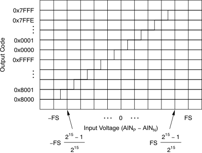
ADS1118 ai_transfer_code-vi_bas457.gifFigure 39. ADS1118 Code Transition Diagram