SBAS925A August   2018  – November 2018 ADS1119

PRODUCTION DATA.  

  1. Features
  2. Applications
  3. Description
    1.     Device Images
      1.      Voltage, Current, and Temperature Monitoring Application
  4. Revision History
  5. Pin Configuration and Functions
    1.     Pin Functions
  6. Specifications
    1. 6.1 Absolute Maximum Ratings
    2. 6.2 ESD Ratings
    3. 6.3 Recommended Operating Conditions
    4. 6.4 Thermal Information
    5. 6.5 Electrical Characteristics
    6. 6.6 I2C Timing Requirements
    7. 6.7 I2C Switching Characteristics
    8. 6.8 Typical Characteristics
  7. Parameter Measurement Information
    1. 7.1 Noise Performance
  8. Detailed Description
    1. 8.1 Overview
    2. 8.2 Functional Block Diagram
    3. 8.3 Feature Description
      1. 8.3.1 Multiplexer
      2. 8.3.2 Rail-to-Rail Input Buffers and Programmable Gain Stage
      3. 8.3.3 Voltage Reference
      4. 8.3.4 Modulator and Internal Oscillator
      5. 8.3.5 Digital Filter
      6. 8.3.6 Conversion Times
      7. 8.3.7 Offset Calibration
    4. 8.4 Device Functional Modes
      1. 8.4.1 Power-Up and Reset
        1. 8.4.1.1 Power-On Reset
        2. 8.4.1.2 RESET Pin
        3. 8.4.1.3 Reset by Command
      2. 8.4.2 Conversion Modes
        1. 8.4.2.1 Single-Shot Conversion Mode
        2. 8.4.2.2 Continuous Conversion Mode
      3. 8.4.3 Power-Down Mode
    5. 8.5 Programming
      1. 8.5.1 I2C Interface
        1. 8.5.1.1 I2C Address
        2. 8.5.1.2 Serial Clock (SCL) and Serial Data (SDA)
        3. 8.5.1.3 Data Ready (DRDY)
        4. 8.5.1.4 Interface Speed
        5. 8.5.1.5 Data Transfer Protocol
        6. 8.5.1.6 I2C General Call (Software Reset)
        7. 8.5.1.7 Timeout
      2. 8.5.2 Data Format
      3. 8.5.3 Commands
        1. 8.5.3.1 Command Latching
        2. 8.5.3.2 RESET (0000 011x)
        3. 8.5.3.3 START/SYNC (0000 100x)
        4. 8.5.3.4 POWERDOWN (0000 001x)
        5. 8.5.3.5 RDATA (0001 xxxx)
        6. 8.5.3.6 RREG (0010 0rxx)
        7. 8.5.3.7 WREG (0100 00xx dddd dddd)
      4. 8.5.4 Reading Data and Monitoring for New Conversion Results
    6. 8.6 Register Map
      1. 8.6.1 Configuration and Status Registers
      2. 8.6.2 Register Descriptions
        1. 8.6.2.1 Configuration Register (address = 0h) [reset = 00h]
          1. Table 10. Configuration Register Field Descriptions
        2. 8.6.2.2 Status Register (address = 1h) [reset = 00h]
          1. Table 11. Status Register Field Descriptions
  9. Application and Implementation
    1. 9.1 Application Information
      1. 9.1.1 Interface Connections
      2. 9.1.2 Connecting Multiple Devices on the Same I2C Bus
      3. 9.1.3 Unused Inputs and Outputs
      4. 9.1.4 Analog Input Filtering
      5. 9.1.5 External Reference and Ratiometric Measurements
      6. 9.1.6 Establishing Proper Limits on the Absolute Input Voltage
      7. 9.1.7 Pseudo Code Example
    2. 9.2 Typical Application
      1. 9.2.1 Design Requirements
      2. 9.2.2 Detailed Design Procedure
        1. 9.2.2.1 Voltage Monitoring
        2. 9.2.2.2 High-Side Current Measurement
        3. 9.2.2.3 Thermistor Measurement
        4. 9.2.2.4 Register Settings
      3. 9.2.3 Application Curve
  10. 10Power Supply Recommendations
    1. 10.1 Power-Supply Sequencing
    2. 10.2 Power-Supply Decoupling
  11. 11Layout
    1. 11.1 Layout Guidelines
    2. 11.2 Layout Example
  12. 12Device and Documentation Support
    1. 12.1 Device Support
      1. 12.1.1 Third-Party Products Disclaimer
    2. 12.2 Documentation Support
      1. 12.2.1 Related Documentation
    3. 12.3 Receiving Notification of Documentation Updates
    4. 12.4 Community Resources
    5. 12.5 Trademarks
    6. 12.6 Electrostatic Discharge Caution
    7. 12.7 Glossary
  13. 13Mechanical, Packaging, and Orderable Information

Package Options

Mechanical Data (Package|Pins)
Thermal pad, mechanical data (Package|Pins)
Orderable Information

Typical Characteristics

at TA = 25°C, AVDD = 3.3 V, and using internal VREF = 2.048 V (unless otherwise noted)
ADS1119 D019_sbas752.gif
VIN = 0 V
Figure 4. Absolute Input current vs Absolute Input Voltage
ADS1119 D002_sbas924.gif
External reference, best fit
Figure 6. INL vs Differential Input Voltage
ADS1119 D067_sbas924.gif
AVDD = 5 V, gain = 1, 110 samples
Figure 8. Offset Voltage Histogram
ADS1119 D008_sbas752.gif
Gain = 1, 620 samples,
excluding error of voltage reference
Figure 10. Gain Error Histogram
ADS1119 D051_sbas924.gif
Figure 12. DC CMRR vs Temperature
ADS1119 D063_sbas752.gif
Figure 14. Internal Reference Voltage vs Temperature
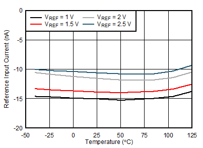
ADS1119 D059_sbas752.gif
Figure 16. External Reference Input Current vs Temperature
ADS1119 D060_sbas752.gif
Figure 18. Internal Oscillator Frequency vs Temperature
ADS1119 vol_vs_iol_bas751.gif
DVDD = 3.3 V
Figure 20. Digital Pin Output Voltage vs Sinking Current
ADS1119 D045_sbas924.gif
Conversion mode
Figure 22. Analog Supply Current vs Temperature
ADS1119 D039_sbas752.gif
Power-down mode
Figure 24. Digital Supply Current vs Temperature
ADS1119 D038_sbas752.gif
Conversion mode
Figure 26. Digital Supply Current vs DVDD
ADS1119 D027_sbas752.gif
VCM = 1.65 V
Figure 5. Differential Input Current vs
Differential Input Voltage
ADS1119 D003_sbas924.gif
Internal reference, best fit
Figure 7. INL vs Differential Input Voltage
ADS1119 D001_sbas924.gif
Figure 9. Input Offset Voltage vs Temperature
ADS1119 D041_sbas924.gif
Excluding error of voltage reference
Figure 11. Gain Error vs Temperature
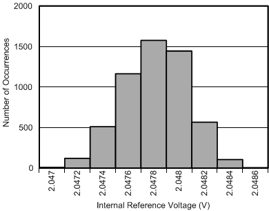
ADS1119 D062_sbas752.gif
5940 samples, TSSOP package
Figure 13. Internal Reference Voltage Histogram
ADS1119 D035_sbas752.gif
Figure 15. Internal Reference Voltage vs AVDD
ADS1119 D053_sbas752.gif
Figure 17. Internal Oscillator Frequency Histogram
ADS1119 D061_sbas752.gif
Figure 19. Internal Oscillator Frequency vs DVDD
ADS1119 D044_sbas752.gif
Power-down mode
Figure 21. Analog Supply Current vs Temperature
ADS1119 D046_sbas924.gif
Conversion mode
Figure 23. Analog Supply Current vs AVDD
ADS1119 D040_sbas752.gif
Conversion mode
Figure 25. Digital Supply Current vs Temperature