SBAS683B August   2014  – May 2020 ADS1120-Q1

PRODUCTION DATA.  

  1. Features
  2. Applications
  3. Description
    1.     Device Images
      1.      Block Diagram
  4. Revision History
  5. Pin Configuration and Functions
    1.     Pin Functions
  6. Specifications
    1. 6.1 Absolute Maximum Ratings
    2. 6.2 ESD Ratings
    3. 6.3 Recommended Operating Conditions
    4. 6.4 Thermal Information
    5. 6.5 Electrical Characteristics
    6. 6.6 SPI Timing Requirements
    7. 6.7 SPI Switching Characteristics
    8. 6.8 Typical Characteristics
  7. Parameter Measurement Information
    1. 7.1 Noise Performance
  8. Detailed Description
    1. 8.1 Overview
    2. 8.2 Functional Block Diagram
    3. 8.3 Feature Description
      1. 8.3.1  Multiplexer
      2. 8.3.2  Low-Noise PGA
        1. 8.3.2.1 PGA Common-Mode Voltage Requirements
        2. 8.3.2.2 Bypassing the PGA
      3. 8.3.3  Modulator
      4. 8.3.4  Digital Filter
      5. 8.3.5  Output Data Rate
      6. 8.3.6  Voltage Reference
      7. 8.3.7  Clock Source
      8. 8.3.8  Excitation Current Sources
      9. 8.3.9  Low-Side Power Switch
      10. 8.3.10 Sensor Detection
      11. 8.3.11 System Monitor
      12. 8.3.12 Offset Calibration
      13. 8.3.13 Power Supplies
      14. 8.3.14 Temperature Sensor
        1. 8.3.14.1 Converting from Temperature to Digital Codes
          1. 8.3.14.1.1 For Positive Temperatures (for Example, 50°C):
          2. 8.3.14.1.2 For Negative Temperatures (for Example, –25°C):
        2. 8.3.14.2 Converting from Digital Codes to Temperature
    4. 8.4 Device Functional Modes
      1. 8.4.1 Power-Up and Reset
      2. 8.4.2 Conversion Modes
        1. 8.4.2.1 Single-Shot Mode
        2. 8.4.2.2 Continuous-Conversion Mode
      3. 8.4.3 Operating Modes
        1. 8.4.3.1 Normal Mode
        2. 8.4.3.2 Duty-Cycle Mode
        3. 8.4.3.3 Turbo Mode
        4. 8.4.3.4 Power-Down Mode
    5. 8.5 Programming
      1. 8.5.1 Serial Interface
        1. 8.5.1.1 Chip Select (CS)
        2. 8.5.1.2 Serial Clock (SCLK)
        3. 8.5.1.3 Data Ready (DRDY)
        4. 8.5.1.4 Data Input (DIN)
        5. 8.5.1.5 Data Output and Data Ready (DOUT/DRDY)
        6. 8.5.1.6 SPI Timeout
      2. 8.5.2 Data Format
      3. 8.5.3 Commands
        1. 8.5.3.1 RESET (0000 011x)
        2. 8.5.3.2 START/SYNC (0000 100x)
        3. 8.5.3.3 POWERDOWN (0000 001x)
        4. 8.5.3.4 RDATA (0001 xxxx)
        5. 8.5.3.5 RREG (0010 rrnn)
        6. 8.5.3.6 WREG (0100 rrnn)
      4. 8.5.4 Reading Data
      5. 8.5.5 Sending Commands
      6. 8.5.6 Interfacing with Multiple Devices
    6. 8.6 Register Map
      1. 8.6.1 Configuration Registers
        1. 8.6.1.1 Configuration Register 0 (Address = 00h) [reset = 00h]
          1. Table 12. Configuration Register 0 Field Descriptions
        2. 8.6.1.2 Configuration Register 1 (Address = 01h) [reset = 00h]
          1. Table 13. Configuration Register 1 Field Descriptions
        3. 8.6.1.3 Configuration Register 2 (Address = 02h) [reset = 00h]
          1. Table 15. Configuration Register 2 Field Descriptions
        4. 8.6.1.4 Configuration Register 3 (Address = 03h) [reset = 00h]
          1. Table 16. Configuration Register 3 Field Descriptions
  9. Application and Implementation
    1. 9.1 Application Information
      1. 9.1.1 Serial Interface Connections
      2. 9.1.2 Analog Input Filtering
      3. 9.1.3 External Reference and Ratiometric Measurements
      4. 9.1.4 Establishing a Proper Common-Mode Input Voltage
      5. 9.1.5 Unused Inputs and Outputs
      6. 9.1.6 Pseudo Code Example
    2. 9.2 Typical Applications
      1. 9.2.1 K-Type Thermocouple Measurement (–200°C to +1250°C)
        1. 9.2.1.1 Design Requirements
        2. 9.2.1.2 Detailed Design Procedure
        3. 9.2.1.3 Application Curves
      2. 9.2.2 3-Wire RTD Measurement (–200°C to +850°C)
        1. 9.2.2.1 Design Requirements
        2. 9.2.2.2 Detailed Design Procedure
          1. 9.2.2.2.1 Design Variations for 2-Wire and 4-Wire RTD Measurements
        3. 9.2.2.3 Application Curves
      3. 9.2.3 Bridge Measurement
        1. 9.2.3.1 Design Requirements
        2. 9.2.3.2 Detailed Design Procedure
  10. 10Power Supply Recommendations
    1. 10.1 Power-Supply Sequencing
    2. 10.2 Power-Supply Ramp Rate
    3. 10.3 Power-Supply Decoupling
  11. 11Layout
    1. 11.1 Layout Guidelines
    2. 11.2 Layout Example
  12. 12Device and Documentation Support
    1. 12.1 Documentation Support
      1. 12.1.1 Related Documentation
    2. 12.2 Receiving Notification of Documentation Updates
    3. 12.3 Support Resources
    4. 12.4 Trademarks
    5. 12.5 Electrostatic Discharge Caution
    6. 12.6 Glossary
  13. 13Mechanical, Packaging, and Orderable Information

Package Options

Mechanical Data (Package|Pins)
Thermal pad, mechanical data (Package|Pins)
Orderable Information

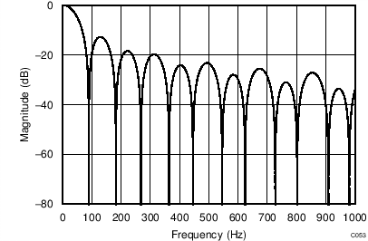
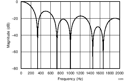
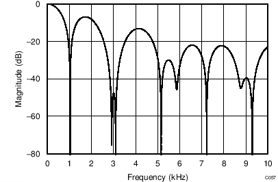
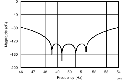
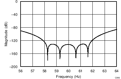
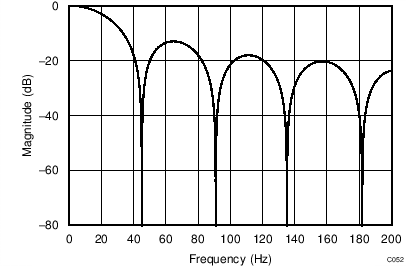
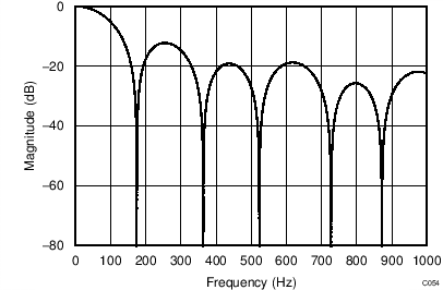
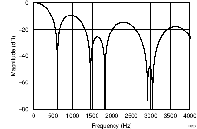
Digital Filter

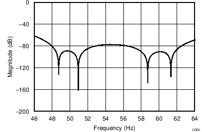
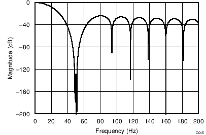
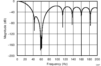
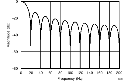
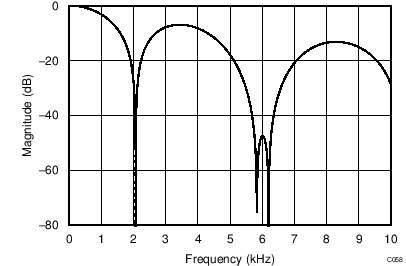
The device uses a linear-phase finite impulse response (FIR) digital filter that performs both filtering and decimation of the digital data stream coming from the modulator. The digital filter is automatically adjusted for the different data rates and always settles within a single cycle. At data rates of 5 SPS and 20 SPS, the filter can be configured to reject 50-Hz or 60-Hz line frequencies or to simultaneously reject 50 Hz and 60 Hz. Two bits (50/60[1:0]) in the configuration register are used to configure the filter accordingly. The frequency responses of the digital filter are shown in Figure 46 to Figure 59 for different output data rates using the internal oscillator or an external 4.096-MHz clock.

The filter notches and output data rate scale proportionally with the clock frequency. For example, a notch that appears at 20 Hz when using a 4.096-MHz clock appears at 10 Hz if a 2.048-MHz clock is used. Note that the internal oscillator can vary over temperature as specified in the Electrical Characteristics table. The data rate or conversion time, respectively, and filter notches consequently vary by the same amount. Consider using an external precision clock source if a digital filter notch at a specific frequency with a tighter tolerance is required.
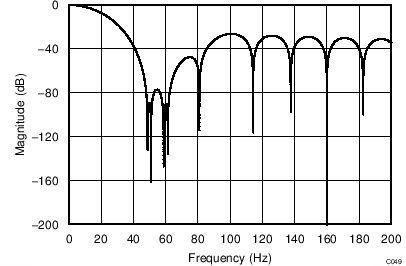
ADS1120-Q1 C049_filter_20SPS_5060Hz_bas501.png
Simultaneous 50-Hz and 60-Hz Rejection, 50/60[1:0] = 01
Figure 46. Filter Response
(DR = 20 SPS)
ADS1120-Q1 C050_20SPS_5060Hz_zoomed_bas501.png
Simultaneous 50-Hz and 60-Hz Rejection, 50/60[1:0] = 01
Figure 47. Detailed View of Filter Response
(DR = 20 SPS)
ADS1120-Q1 C045_20SPS_50Hz_bas501.png
50-Hz Rejection Only, 50/60[1:0] = 10
Figure 48. Filter Response
(DR = 20 SPS)
ADS1120-Q1 C047_filter_20SPS_60Hz_bas501.png
60-Hz Rejection Only, 50/60[1:0] = 11
Figure 50. Filter Response
(DR = 20 SPS)
ADS1120-Q1 C051_20SPS_No_5060Hz_bas501.png
50/60[1:0] = 00
Figure 52. Filter Response
(DR = 20 SPS)
ADS1120-Q1 C053_filter_90SPS_bas501.png
Figure 54. Filter Response
(DR = 90 SPS)
ADS1120-Q1 C055_filter_330SPS_bas501.png
Figure 56. Filter Response
(DR = 330 SPS)
ADS1120-Q1 C057_filter_1kSPS_bas501.png
Figure 58. Filter Response
(DR = 1 kSPS)
ADS1120-Q1 C046_20SPS_50Hz_zoomed_bas501.png
50-Hz Rejection Only, 50/60[1:0] = 10
Figure 49. Detailed View of Filter Response
(DR = 20 SPS)
ADS1120-Q1 C048_20SPS_60Hz_zoomed_bas501.png
60-Hz Rejection Only, 50/60[1:0] = 11
Figure 51. Detailed View of Filter Response
(DR = 20 SPS)
ADS1120-Q1 C052_filter_45SPS_bas501.png
Figure 53. Filter Response
(DR = 45 SPS)
ADS1120-Q1 C054_filter_175SPS_bas501.png
Figure 55. Filter Response
(DR = 175 SPS)
ADS1120-Q1 C056_filter_600SPS_bas501.png
Figure 57. Filter Response
(DR = 600 SPS)
ADS1120-Q1 C058_filter_2kSPS_bas501.png
Figure 59. Filter Response
(DR = 2 kSPS)