SBAS683B
August 2014 – May 2020
ADS1120-Q1
PRODUCTION DATA.
1
Features
2
Applications
3
Description
Device Images
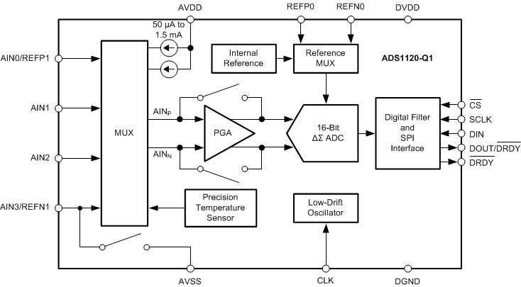
Block Diagram
4
Revision History
5
Pin Configuration and Functions
Pin Functions
6
Specifications
6.1
Absolute Maximum Ratings
6.2
ESD Ratings
6.3
Recommended Operating Conditions
6.4
Thermal Information
6.5
Electrical Characteristics
6.6
SPI Timing Requirements
6.7
SPI Switching Characteristics
6.8
Typical Characteristics
7
Parameter Measurement Information
7.1
Noise Performance
8
Detailed Description
8.1
Overview
8.2
Functional Block Diagram
8.3
Feature Description
8.3.1
Multiplexer
8.3.2
Low-Noise PGA
8.3.2.1
PGA Common-Mode Voltage Requirements
8.3.2.2
Bypassing the PGA
8.3.3
Modulator
8.3.4
Digital Filter
8.3.5
Output Data Rate
8.3.6
Voltage Reference
8.3.7
Clock Source
8.3.8
Excitation Current Sources
8.3.9
Low-Side Power Switch
8.3.10
Sensor Detection
8.3.11
System Monitor
8.3.12
Offset Calibration
8.3.13
Power Supplies
8.3.14
Temperature Sensor
8.3.14.1
Converting from Temperature to Digital Codes
8.3.14.1.1
For Positive Temperatures (for Example, 50°C):
8.3.14.1.2
For Negative Temperatures (for Example, –25°C):
8.3.14.2
Converting from Digital Codes to Temperature
8.4
Device Functional Modes
8.4.1
Power-Up and Reset
8.4.2
Conversion Modes
8.4.2.1
Single-Shot Mode
8.4.2.2
Continuous-Conversion Mode
8.4.3
Operating Modes
8.4.3.1
Normal Mode
8.4.3.2
Duty-Cycle Mode
8.4.3.3
Turbo Mode
8.4.3.4
Power-Down Mode
8.5
Programming
8.5.1
Serial Interface
8.5.1.1
Chip Select (CS)
8.5.1.2
Serial Clock (SCLK)
8.5.1.3
Data Ready (DRDY)
8.5.1.4
Data Input (DIN)
8.5.1.5
Data Output and Data Ready (DOUT/DRDY)
8.5.1.6
SPI Timeout
8.5.2
Data Format
8.5.3
Commands
8.5.3.1
RESET (0000 011x)
8.5.3.2
START/SYNC (0000 100x)
8.5.3.3
POWERDOWN (0000 001x)
8.5.3.4
RDATA (0001 xxxx)
8.5.3.5
RREG (0010 rrnn)
8.5.3.6
WREG (0100 rrnn)
8.5.4
Reading Data
8.5.5
Sending Commands
8.5.6
Interfacing with Multiple Devices
8.6
Register Map
8.6.1
Configuration Registers
8.6.1.1
Configuration Register 0 (Address = 00h) [reset = 00h]
Table 12.
Configuration Register 0 Field Descriptions
8.6.1.2
Configuration Register 1 (Address = 01h) [reset = 00h]
Table 13.
Configuration Register 1 Field Descriptions
8.6.1.3
Configuration Register 2 (Address = 02h) [reset = 00h]
Table 15.
Configuration Register 2 Field Descriptions
8.6.1.4
Configuration Register 3 (Address = 03h) [reset = 00h]
Table 16.
Configuration Register 3 Field Descriptions
9
Application and Implementation
9.1
Application Information
9.1.1
Serial Interface Connections
9.1.2
Analog Input Filtering
9.1.3
External Reference and Ratiometric Measurements
9.1.4
Establishing a Proper Common-Mode Input Voltage
9.1.5
Unused Inputs and Outputs
9.1.6
Pseudo Code Example
9.2
Typical Applications
9.2.1
K-Type Thermocouple Measurement (–200°C to +1250°C)
9.2.1.1
Design Requirements
9.2.1.2
Detailed Design Procedure
9.2.1.3
Application Curves
9.2.2
3-Wire RTD Measurement (–200°C to +850°C)
9.2.2.1
Design Requirements
9.2.2.2
Detailed Design Procedure
9.2.2.2.1
Design Variations for 2-Wire and 4-Wire RTD Measurements
9.2.2.3
Application Curves
9.2.3
Bridge Measurement
9.2.3.1
Design Requirements
9.2.3.2
Detailed Design Procedure
10
Power Supply Recommendations
10.1
Power-Supply Sequencing
10.2
Power-Supply Ramp Rate
10.3
Power-Supply Decoupling
11
Layout
11.1
Layout Guidelines
11.2
Layout Example
12
Device and Documentation Support
12.1
Documentation Support
12.1.1
Related Documentation
12.2
Receiving Notification of Documentation Updates
12.3
Support Resources
12.4
Trademarks
12.5
Electrostatic Discharge Caution
12.6
Glossary
13
Mechanical, Packaging, and Orderable Information
Package Options
Mechanical Data (Package|Pins)
PW|16
MPDS361A
Thermal pad, mechanical data (Package|Pins)
Orderable Information
sbas683b_oa
sbas683b_pm
8.2
Functional Block Diagram