SBAS683B August 2014 – May 2020 ADS1120-Q1
PRODUCTION DATA.
- 1 Features
- 2 Applications
- 3 Description
- 4 Revision History
- 5 Pin Configuration and Functions
- 6 Specifications
- 7 Parameter Measurement Information
-
8 Detailed Description
- 8.1 Overview
- 8.2 Functional Block Diagram
- 8.3
Feature Description
- 8.3.1 Multiplexer
- 8.3.2 Low-Noise PGA
- 8.3.3 Modulator
- 8.3.4 Digital Filter
- 8.3.5 Output Data Rate
- 8.3.6 Voltage Reference
- 8.3.7 Clock Source
- 8.3.8 Excitation Current Sources
- 8.3.9 Low-Side Power Switch
- 8.3.10 Sensor Detection
- 8.3.11 System Monitor
- 8.3.12 Offset Calibration
- 8.3.13 Power Supplies
- 8.3.14 Temperature Sensor
- 8.4 Device Functional Modes
- 8.5 Programming
- 8.6 Register Map
- 9 Application and Implementation
- 10Power Supply Recommendations
- 11Layout
- 12Device and Documentation Support
- 13Mechanical, Packaging, and Orderable Information
Package Options
Mechanical Data (Package|Pins)
- PW|16
Thermal pad, mechanical data (Package|Pins)
Orderable Information
8.3.2 Low-Noise PGA
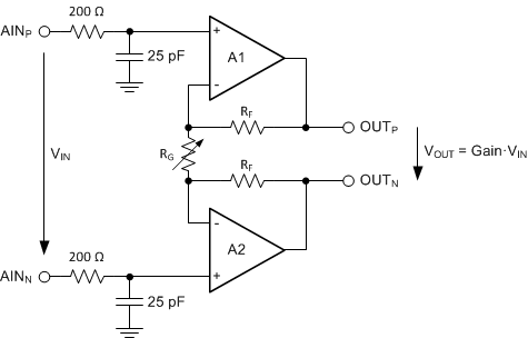
The device features a low-noise, low-drift, high input impedance, programmable gain amplifier (PGA). The PGA can be set to gains of 1, 2, 4, 8, 16, 32, 64, or 128. Three bits (GAIN[2:0]) in the configuration register are used to configure the gain. A simplified diagram of the PGA is shown in Figure 39. The PGA consists of two chopper-stabilized amplifiers (A1 and A2) and a resistor feedback network that sets the PGA gain. The PGA input is equipped with an electromagnetic interference (EMI) filter.
 Figure 39. Simplified PGA Diagram
 VIN denotes the differential input voltage VIN = (V(AINP) – V(AINN)). The gain of the PGA can be calculated with Equation 5:
Gain is changed inside the device using a variable resistor, RG. The differential full-scale input voltage range (FSR) of the PGA is defined by the gain setting and the reference voltage used, as shown in Equation 6:
Table 5 shows the corresponding full-scale ranges when using the internal 2.048-V reference.
Table 5. PGA Full-Scale Range
| GAIN SETTING | FSR |
|---|---|
| 1 | ±2.048 V |
| 2 | ±1.024 V |
| 4 | ±0.512 V |
| 8 | ±0.256 V |
| 16 | ±0.128 V |
| 32 | ±0.064 V |
| 64 | ±0.032 V |
| 128 | ±0.016 V |