SBAS683B August   2014  – May 2020 ADS1120-Q1

PRODUCTION DATA.  

  1. Features
  2. Applications
  3. Description
    1.     Device Images
      1.      Block Diagram
  4. Revision History
  5. Pin Configuration and Functions
    1.     Pin Functions
  6. Specifications
    1. 6.1 Absolute Maximum Ratings
    2. 6.2 ESD Ratings
    3. 6.3 Recommended Operating Conditions
    4. 6.4 Thermal Information
    5. 6.5 Electrical Characteristics
    6. 6.6 SPI Timing Requirements
    7. 6.7 SPI Switching Characteristics
    8. 6.8 Typical Characteristics
  7. Parameter Measurement Information
    1. 7.1 Noise Performance
  8. Detailed Description
    1. 8.1 Overview
    2. 8.2 Functional Block Diagram
    3. 8.3 Feature Description
      1. 8.3.1  Multiplexer
      2. 8.3.2  Low-Noise PGA
        1. 8.3.2.1 PGA Common-Mode Voltage Requirements
        2. 8.3.2.2 Bypassing the PGA
      3. 8.3.3  Modulator
      4. 8.3.4  Digital Filter
      5. 8.3.5  Output Data Rate
      6. 8.3.6  Voltage Reference
      7. 8.3.7  Clock Source
      8. 8.3.8  Excitation Current Sources
      9. 8.3.9  Low-Side Power Switch
      10. 8.3.10 Sensor Detection
      11. 8.3.11 System Monitor
      12. 8.3.12 Offset Calibration
      13. 8.3.13 Power Supplies
      14. 8.3.14 Temperature Sensor
        1. 8.3.14.1 Converting from Temperature to Digital Codes
          1. 8.3.14.1.1 For Positive Temperatures (for Example, 50°C):
          2. 8.3.14.1.2 For Negative Temperatures (for Example, –25°C):
        2. 8.3.14.2 Converting from Digital Codes to Temperature
    4. 8.4 Device Functional Modes
      1. 8.4.1 Power-Up and Reset
      2. 8.4.2 Conversion Modes
        1. 8.4.2.1 Single-Shot Mode
        2. 8.4.2.2 Continuous-Conversion Mode
      3. 8.4.3 Operating Modes
        1. 8.4.3.1 Normal Mode
        2. 8.4.3.2 Duty-Cycle Mode
        3. 8.4.3.3 Turbo Mode
        4. 8.4.3.4 Power-Down Mode
    5. 8.5 Programming
      1. 8.5.1 Serial Interface
        1. 8.5.1.1 Chip Select (CS)
        2. 8.5.1.2 Serial Clock (SCLK)
        3. 8.5.1.3 Data Ready (DRDY)
        4. 8.5.1.4 Data Input (DIN)
        5. 8.5.1.5 Data Output and Data Ready (DOUT/DRDY)
        6. 8.5.1.6 SPI Timeout
      2. 8.5.2 Data Format
      3. 8.5.3 Commands
        1. 8.5.3.1 RESET (0000 011x)
        2. 8.5.3.2 START/SYNC (0000 100x)
        3. 8.5.3.3 POWERDOWN (0000 001x)
        4. 8.5.3.4 RDATA (0001 xxxx)
        5. 8.5.3.5 RREG (0010 rrnn)
        6. 8.5.3.6 WREG (0100 rrnn)
      4. 8.5.4 Reading Data
      5. 8.5.5 Sending Commands
      6. 8.5.6 Interfacing with Multiple Devices
    6. 8.6 Register Map
      1. 8.6.1 Configuration Registers
        1. 8.6.1.1 Configuration Register 0 (Address = 00h) [reset = 00h]
          1. Table 12. Configuration Register 0 Field Descriptions
        2. 8.6.1.2 Configuration Register 1 (Address = 01h) [reset = 00h]
          1. Table 13. Configuration Register 1 Field Descriptions
        3. 8.6.1.3 Configuration Register 2 (Address = 02h) [reset = 00h]
          1. Table 15. Configuration Register 2 Field Descriptions
        4. 8.6.1.4 Configuration Register 3 (Address = 03h) [reset = 00h]
          1. Table 16. Configuration Register 3 Field Descriptions
  9. Application and Implementation
    1. 9.1 Application Information
      1. 9.1.1 Serial Interface Connections
      2. 9.1.2 Analog Input Filtering
      3. 9.1.3 External Reference and Ratiometric Measurements
      4. 9.1.4 Establishing a Proper Common-Mode Input Voltage
      5. 9.1.5 Unused Inputs and Outputs
      6. 9.1.6 Pseudo Code Example
    2. 9.2 Typical Applications
      1. 9.2.1 K-Type Thermocouple Measurement (–200°C to +1250°C)
        1. 9.2.1.1 Design Requirements
        2. 9.2.1.2 Detailed Design Procedure
        3. 9.2.1.3 Application Curves
      2. 9.2.2 3-Wire RTD Measurement (–200°C to +850°C)
        1. 9.2.2.1 Design Requirements
        2. 9.2.2.2 Detailed Design Procedure
          1. 9.2.2.2.1 Design Variations for 2-Wire and 4-Wire RTD Measurements
        3. 9.2.2.3 Application Curves
      3. 9.2.3 Bridge Measurement
        1. 9.2.3.1 Design Requirements
        2. 9.2.3.2 Detailed Design Procedure
  10. 10Power Supply Recommendations
    1. 10.1 Power-Supply Sequencing
    2. 10.2 Power-Supply Ramp Rate
    3. 10.3 Power-Supply Decoupling
  11. 11Layout
    1. 11.1 Layout Guidelines
    2. 11.2 Layout Example
  12. 12Device and Documentation Support
    1. 12.1 Documentation Support
      1. 12.1.1 Related Documentation
    2. 12.2 Receiving Notification of Documentation Updates
    3. 12.3 Support Resources
    4. 12.4 Trademarks
    5. 12.5 Electrostatic Discharge Caution
    6. 12.6 Glossary
  13. 13Mechanical, Packaging, and Orderable Information

Package Options

Mechanical Data (Package|Pins)
Thermal pad, mechanical data (Package|Pins)
Orderable Information

Serial Interface Connections

The principle serial interface connections for the ADS1120-Q1 are shown in Figure 72.
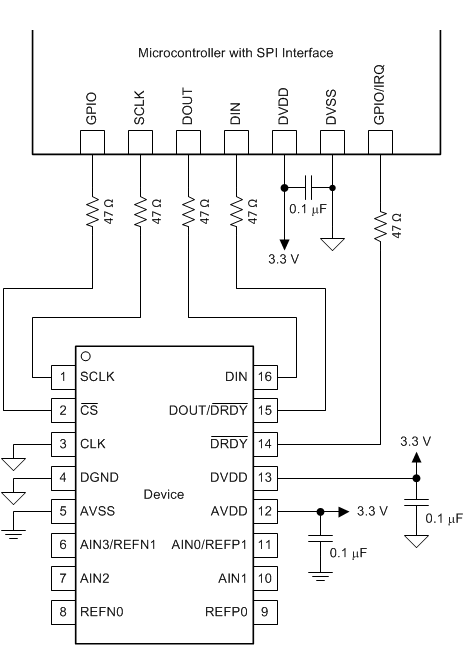
ADS1120-Q1 ai_mcu_connection_bas683.gifFigure 72. Serial Interface Connections

Most microcontroller SPI peripherals can operate with the ADS1120-Q1. The interface operates in SPI mode 1 where CPOL = 0 and CPHA = 1. In SPI mode 1, SCLK idles low and data are launched or changed only on SCLK rising edges; data are latched or read by the master and slave on SCLK falling edges. Details of the SPI communication protocol employed by the device can be found in the SPI Timing Requirements section.

TI recommends placing 47-Ω resistors in series with all digital input and output pins (CS, SCLK, DIN, DOUT/DRDY, and DRDY). This resistance smooths sharp transitions, suppresses overshoot, and offers some overvoltage protection. Care must be taken to meet all SPI timing requirements because the additional resistors interact with the bus capacitances present on the digital signal lines.