SBAS683B August   2014  – May 2020 ADS1120-Q1

PRODUCTION DATA.  

  1. Features
  2. Applications
  3. Description
    1.     Device Images
      1.      Block Diagram
  4. Revision History
  5. Pin Configuration and Functions
    1.     Pin Functions
  6. Specifications
    1. 6.1 Absolute Maximum Ratings
    2. 6.2 ESD Ratings
    3. 6.3 Recommended Operating Conditions
    4. 6.4 Thermal Information
    5. 6.5 Electrical Characteristics
    6. 6.6 SPI Timing Requirements
    7. 6.7 SPI Switching Characteristics
    8. 6.8 Typical Characteristics
  7. Parameter Measurement Information
    1. 7.1 Noise Performance
  8. Detailed Description
    1. 8.1 Overview
    2. 8.2 Functional Block Diagram
    3. 8.3 Feature Description
      1. 8.3.1  Multiplexer
      2. 8.3.2  Low-Noise PGA
        1. 8.3.2.1 PGA Common-Mode Voltage Requirements
        2. 8.3.2.2 Bypassing the PGA
      3. 8.3.3  Modulator
      4. 8.3.4  Digital Filter
      5. 8.3.5  Output Data Rate
      6. 8.3.6  Voltage Reference
      7. 8.3.7  Clock Source
      8. 8.3.8  Excitation Current Sources
      9. 8.3.9  Low-Side Power Switch
      10. 8.3.10 Sensor Detection
      11. 8.3.11 System Monitor
      12. 8.3.12 Offset Calibration
      13. 8.3.13 Power Supplies
      14. 8.3.14 Temperature Sensor
        1. 8.3.14.1 Converting from Temperature to Digital Codes
          1. 8.3.14.1.1 For Positive Temperatures (for Example, 50°C):
          2. 8.3.14.1.2 For Negative Temperatures (for Example, –25°C):
        2. 8.3.14.2 Converting from Digital Codes to Temperature
    4. 8.4 Device Functional Modes
      1. 8.4.1 Power-Up and Reset
      2. 8.4.2 Conversion Modes
        1. 8.4.2.1 Single-Shot Mode
        2. 8.4.2.2 Continuous-Conversion Mode
      3. 8.4.3 Operating Modes
        1. 8.4.3.1 Normal Mode
        2. 8.4.3.2 Duty-Cycle Mode
        3. 8.4.3.3 Turbo Mode
        4. 8.4.3.4 Power-Down Mode
    5. 8.5 Programming
      1. 8.5.1 Serial Interface
        1. 8.5.1.1 Chip Select (CS)
        2. 8.5.1.2 Serial Clock (SCLK)
        3. 8.5.1.3 Data Ready (DRDY)
        4. 8.5.1.4 Data Input (DIN)
        5. 8.5.1.5 Data Output and Data Ready (DOUT/DRDY)
        6. 8.5.1.6 SPI Timeout
      2. 8.5.2 Data Format
      3. 8.5.3 Commands
        1. 8.5.3.1 RESET (0000 011x)
        2. 8.5.3.2 START/SYNC (0000 100x)
        3. 8.5.3.3 POWERDOWN (0000 001x)
        4. 8.5.3.4 RDATA (0001 xxxx)
        5. 8.5.3.5 RREG (0010 rrnn)
        6. 8.5.3.6 WREG (0100 rrnn)
      4. 8.5.4 Reading Data
      5. 8.5.5 Sending Commands
      6. 8.5.6 Interfacing with Multiple Devices
    6. 8.6 Register Map
      1. 8.6.1 Configuration Registers
        1. 8.6.1.1 Configuration Register 0 (Address = 00h) [reset = 00h]
          1. Table 12. Configuration Register 0 Field Descriptions
        2. 8.6.1.2 Configuration Register 1 (Address = 01h) [reset = 00h]
          1. Table 13. Configuration Register 1 Field Descriptions
        3. 8.6.1.3 Configuration Register 2 (Address = 02h) [reset = 00h]
          1. Table 15. Configuration Register 2 Field Descriptions
        4. 8.6.1.4 Configuration Register 3 (Address = 03h) [reset = 00h]
          1. Table 16. Configuration Register 3 Field Descriptions
  9. Application and Implementation
    1. 9.1 Application Information
      1. 9.1.1 Serial Interface Connections
      2. 9.1.2 Analog Input Filtering
      3. 9.1.3 External Reference and Ratiometric Measurements
      4. 9.1.4 Establishing a Proper Common-Mode Input Voltage
      5. 9.1.5 Unused Inputs and Outputs
      6. 9.1.6 Pseudo Code Example
    2. 9.2 Typical Applications
      1. 9.2.1 K-Type Thermocouple Measurement (–200°C to +1250°C)
        1. 9.2.1.1 Design Requirements
        2. 9.2.1.2 Detailed Design Procedure
        3. 9.2.1.3 Application Curves
      2. 9.2.2 3-Wire RTD Measurement (–200°C to +850°C)
        1. 9.2.2.1 Design Requirements
        2. 9.2.2.2 Detailed Design Procedure
          1. 9.2.2.2.1 Design Variations for 2-Wire and 4-Wire RTD Measurements
        3. 9.2.2.3 Application Curves
      3. 9.2.3 Bridge Measurement
        1. 9.2.3.1 Design Requirements
        2. 9.2.3.2 Detailed Design Procedure
  10. 10Power Supply Recommendations
    1. 10.1 Power-Supply Sequencing
    2. 10.2 Power-Supply Ramp Rate
    3. 10.3 Power-Supply Decoupling
  11. 11Layout
    1. 11.1 Layout Guidelines
    2. 11.2 Layout Example
  12. 12Device and Documentation Support
    1. 12.1 Documentation Support
      1. 12.1.1 Related Documentation
    2. 12.2 Receiving Notification of Documentation Updates
    3. 12.3 Support Resources
    4. 12.4 Trademarks
    5. 12.5 Electrostatic Discharge Caution
    6. 12.6 Glossary
  13. 13Mechanical, Packaging, and Orderable Information

Package Options

Mechanical Data (Package|Pins)
Thermal pad, mechanical data (Package|Pins)
Orderable Information

Typical Characteristics

At TA = 25°C, AVDD = 3.3 V, AVSS = 0 V, and PGA enabled using external VREF = 2.5 V (unless otherwise noted).
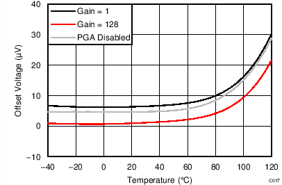
ADS1120-Q1 C017_bas501.png
AVDD = 3.3 V
Figure 3. Input-Referred Offset Voltage vs Temperature
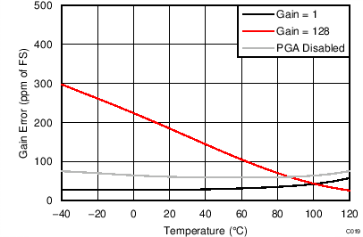
ADS1120-Q1 C019_bas501.png
AVDD = 3.3 V
Figure 5. Gain Error vs Temperature
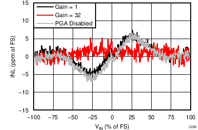
ADS1120-Q1 C025_bas501.png
AVDD = 3.3 V, external 2.5-V reference, normal mode
Figure 7. Integral Nonlinearity vs
Differential Input Signal
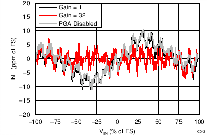
ADS1120-Q1 C043_bas501.png
AVDD = 3.3 V, internal reference, normal mode
Figure 9. Integral Nonlinearity vs
Differential Input Signal
ADS1120-Q1 C042_bas501.png
TA = 25°C, data from 5490 devices
Figure 11. Internal Reference Voltage Histogram
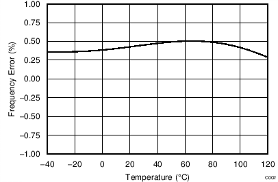
ADS1120-Q1 C002_bas501.png
DVDD = 3.3 V, normal mode
Figure 13. Internal Oscillator Accuracy vs Temperature
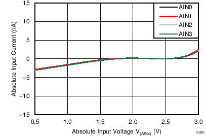
ADS1120-Q1 C030_bas501.png
AVDD = 3.3 V, PGA enabled, TA = –40°C
Figure 15. Absolute Input Current vs
Absolute Input Voltage
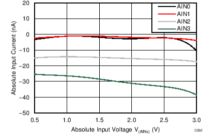
ADS1120-Q1 C032_bas501.png
AVDD = 3.3 V, PGA enabled, TA = 85°C
Figure 17. Absolute Input Current vs
Absolute Input Voltage
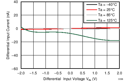
ADS1120-Q1 C038_bas501.png
AVDD = 3.3 V, PGA enabled, AINP = AIN0, AINN = AIN1
Figure 19. Differential Input Current vs
Differential Input Voltage
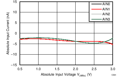
ADS1120-Q1 C034_bas501.png
AVDD = 3.3 V, PGA disabled, TA = –40°C
Figure 21. Absolute Input Current vs
Absolute Input Voltage
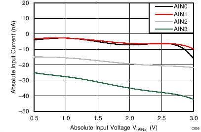
ADS1120-Q1 C036_bas501.png
AVDD = 3.3 V, PGA disabled, TA = 85°C
Figure 23. Absolute Input Current vs
Absolute Input Voltage
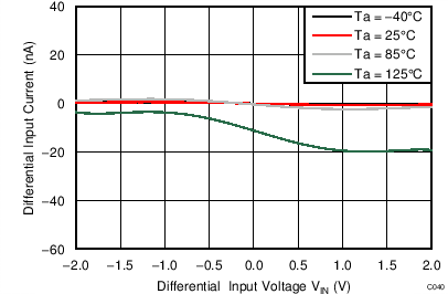
ADS1120-Q1 C040_bas501.png
AVDD = 3.3 V, PGA disabled, AINP = AIN0, AINN = AIN1
Figure 25. Differential Input Current vs
Differential Input Voltage
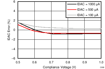
ADS1120-Q1 C006_bas501.png
Figure 27. IDAC Accuracy vs Compliance Voltage
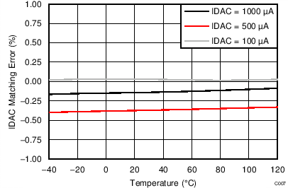
ADS1120-Q1 C007_bas501.png
Figure 29. IDAC Matching vs Temperature
ADS1120-Q1 C012_bas501.png
AVDD = 3.3 V, internal reference, turbo mode
Figure 31. IAVDD vs Temperature
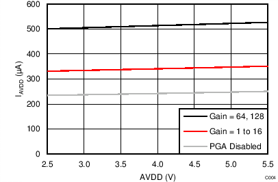
ADS1120-Q1 C004_bas501.png
Normal mode, internal reference
Figure 33. IAVDD vs AVDD
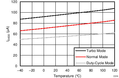
ADS1120-Q1 C014_bas501.png
DVDD = 3.3 V
Figure 35. IDVDD vs Temperature
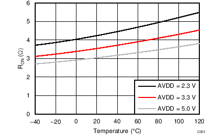
ADS1120-Q1 C001_bas501.png
Figure 37. Low-Side Power Switch RON vs Temperature
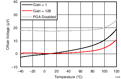
ADS1120-Q1 C018_bas501.png
AVDD = 5.0 V
Figure 4. Input-Referred Offset Voltage vs Temperature
ADS1120-Q1 C020_bas501.png
AVDD = 5.0 V
Figure 6. Gain Error vs Temperature
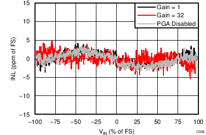
ADS1120-Q1 C029_bas501.png
AVDD = 5.0 V, external 2.5-V reference, normal mode
Figure 8. Integral Nonlinearity vs
Differential Input Signal
ADS1120-Q1 C044_bas501.png
AVDD = 5.0 V, internal reference, normal mode
Figure 10. Integral Nonlinearity vs
Differential Input Signal
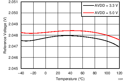
ADS1120-Q1 C021_bas501.png
Figure 12. Internal Reference Voltage vs Temperature
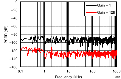
ADS1120-Q1 C016_bas501.png
Figure 14. AVDD Power-Supply Rejection Ratio vs Frequency
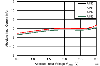
ADS1120-Q1 C031_bas501.png
AVDD = 3.3 V, PGA enabled, TA = 25°C
Figure 16. Absolute Input Current vs
Absolute Input Voltage
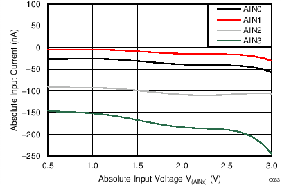
ADS1120-Q1 C033_bas501.png
AVDD = 3.3 V, PGA enabled, TA = 125°C
Figure 18. Absolute Input Current vs
Absolute Input Voltage
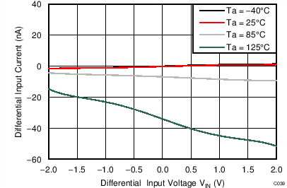
ADS1120-Q1 C039_bas501.png
AVDD = 3.3 V, PGA enabled, AINP = AIN3, AINN = AIN2
Figure 20. Differential Input Current vs
Differential Input Voltage
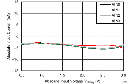
ADS1120-Q1 C035_bas501.png
AVDD = 3.3 V, PGA disabled, TA = 25°C
Figure 22. Absolute Input Current vs
Absolute Input Voltage
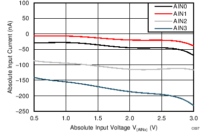
ADS1120-Q1 C037_bas501.png
AVDD = 3.3 V, PGA disabled, TA = 125°C
Figure 24. Absolute Input Current vs
Absolute Input Voltage
ADS1120-Q1 C041_bas501.png
AVDD = 3.3 V, PGA disabled, AINP = AIN3, AINN = AIN2
Figure 26. Differential Input Current vs
Differential Input Voltage
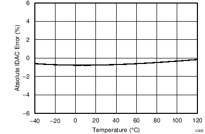
ADS1120-Q1 C005_bas501.png
Figure 28. IDAC Accuracy vs Temperature
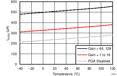
ADS1120-Q1 C011_bas501.png
AVDD = 3.3 V, internal reference, normal mode
Figure 30. IAVDD vs Temperature
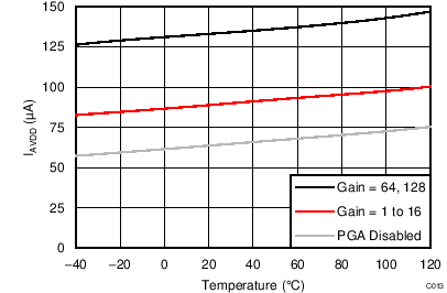
ADS1120-Q1 C013_bas501.png
AVDD = 3.3 V, internal reference, duty-cycle mode
Figure 32. IAVDD vs Temperature
ADS1120-Q1 C010_bas501.png
Figure 34. IDVDD vs DVDD
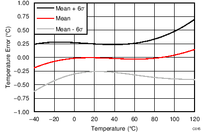
ADS1120-Q1 C015_bas501.png
Figure 36. Internal Temperature Sensor Accuracy vs Temperature