SBAS838A
January 2018 – October 2018
ADS112U04
PRODUCTION DATA.
1
Features
2
Applications
3
Description
Device Images
K-Type Thermocouple Measurement
4
Revision History
5
Pin Configuration and Functions
Pin Functions
6
Specifications
6.1
Absolute Maximum Ratings
6.2
ESD Ratings
6.3
Recommended Operating Conditions
6.4
Thermal Information
6.5
Electrical Characteristics
6.6
UART Timing Requirements
6.7
UART Switching Characteristics
6.8
Typical Characteristics
7
Parameter Measurement Information
7.1
Noise Performance
8
Detailed Description
8.1
Overview
8.2
Functional Block Diagram
8.3
Feature Description
8.3.1
Multiplexer
8.3.2
Low-Noise Programmable Gain Stage
8.3.2.1
PGA Input Voltage Requirements
8.3.2.2
Bypassing the PGA
8.3.3
Voltage Reference
8.3.4
Modulator and Internal Oscillator
8.3.5
Digital Filter
8.3.6
Conversion Times
8.3.7
Excitation Current Sources
8.3.8
Sensor Detection
8.3.9
System Monitor
8.3.10
Temperature Sensor
8.3.10.1
Converting From Temperature to Digital Codes
8.3.10.1.1
For Positive Temperatures (For Example, 50°C):
8.3.10.1.2
For Negative Temperatures (For Example, –25°C):
8.3.10.2
Converting From Digital Codes to Temperature
8.3.11
Offset Calibration
8.3.12
Conversion Data Counter
8.3.13
Data Integrity
8.3.14
General-Purpose Digital Inputs/Outputs
8.4
Device Functional Modes
8.4.1
Power-Up and Reset
8.4.1.1
Power-On Reset
8.4.1.2
RESET Pin
8.4.1.3
Reset by Command
8.4.2
Conversion Modes
8.4.2.1
Single-Shot Conversion Mode
8.4.2.2
Continuous Conversion Mode
8.4.3
Operating Modes
8.4.3.1
Normal Mode
8.4.3.2
Turbo Mode
8.4.3.3
Power-Down Mode
8.5
Programming
8.5.1
UART Interface
8.5.1.1
Receive (RX)
8.5.1.2
Transmit (TX)
8.5.1.3
Data Ready (DRDY)
8.5.1.4
Protocol
8.5.1.5
Timeout
8.5.2
Data Format
8.5.3
Commands
8.5.3.1
RESET (0000 011x)
8.5.3.2
START/SYNC (0000 100x)
8.5.3.3
POWERDOWN (0000 001x)
8.5.3.4
RDATA (0001 xxxx)
8.5.3.5
RREG (0010 rrrx)
8.5.3.6
WREG (0100 rrrx dddd dddd)
8.5.3.7
Command Latching
8.5.4
Reading Data
8.5.4.1
Manual Data Read Mode
8.5.4.2
Automatic Data Read Mode
8.5.5
Data Integrity
8.6
Register Map
8.6.1
Configuration Registers
8.6.2
Register Descriptions
8.6.2.1
Configuration Register 0 (address = 00h) [reset = 00h]
Table 18.
Configuration Register 0 Field Descriptions
8.6.2.2
Configuration Register 1 (address = 01h) [reset = 00h]
Table 19.
Configuration Register 1 Field Descriptions
8.6.2.3
Configuration Register 2 (address = 02h) [reset = 00h]
Table 21.
Configuration Register 2 Field Descriptions
8.6.2.4
Configuration Register 3 (address = 03h) [reset = 00h]
Table 22.
Configuration Register 3 Field Descriptions
8.6.2.5
Configuration Register 4 (address = 04h) [reset = 00h]
Table 23.
Configuration Register 4 Field Descriptions
9
Application and Implementation
9.1
Application Information
9.1.1
Interface Connections
9.1.2
Analog Input Filtering
9.1.3
External Reference and Ratiometric Measurements
9.1.4
Establishing Proper Limits on the Absolute Input Voltage
9.1.5
Unused Inputs and Outputs
9.1.6
Pseudo Code Example
9.2
Typical Applications
9.2.1
K-Type Thermocouple Measurement (–200°C to +1250°C)
9.2.1.1
Design Requirements
9.2.1.2
Detailed Design Procedure
9.2.1.3
Application Curves
9.2.2
3-Wire RTD Measurement (–200°C to +850°C)
9.2.2.1
Design Requirements
9.2.2.2
Detailed Design Procedure
9.2.2.2.1
Design Variations for 2-Wire and 4-Wire RTD Measurements
9.2.2.3
Application Curves
9.2.3
Resistive Bridge Measurement
9.2.3.1
Design Requirements
9.2.3.2
Detailed Design Procedure
10
Power Supply Recommendations
10.1
Power-Supply Sequencing
10.2
Power-Supply Decoupling
11
Layout
11.1
Layout Guidelines
11.2
Layout Example
12
Device and Documentation Support
12.1
Documentation Support
12.1.1
Related Documentation
12.2
Receiving Notification of Documentation Updates
12.3
Community Resources
12.4
Trademarks
12.5
Electrostatic Discharge Caution
12.6
Glossary
13
Mechanical, Packaging, and Orderable Information
Package Options
Mechanical Data (Package|Pins)
RTE|16
MPQF149D
PW|16
MPDS361A
Thermal pad, mechanical data (Package|Pins)
RTE|16
QFND298F
Orderable Information
sbas838a_oa
sbas838a_pm
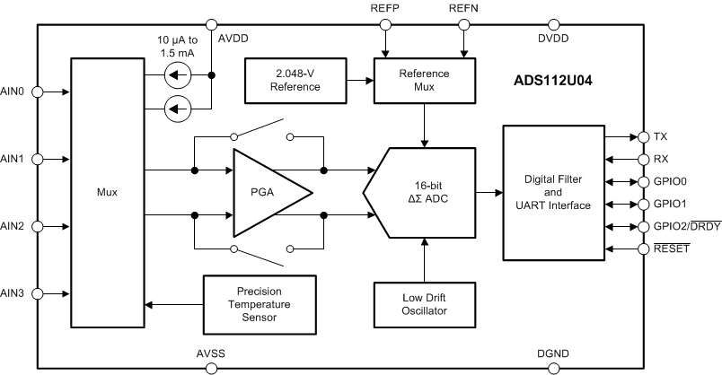
8.2
Functional Block Diagram