SBAS301D October 2003 – February 2020 ADS1204
PRODUCTION DATA.
- 1 Features
- 2 Applications
- 3 Description
- 4 Revision History
- 5 Pin Configuration and Functions
- 6 Specifications
- 7 Detailed Description
- 8 Application and Implementation
- 9 Power Supply Recommendations
- 10Layout
- 11Device and Documentation Support
- 12Mechanical, Packaging, and Orderable Information
Package Options
Mechanical Data (Package|Pins)
- RHB|32
Thermal pad, mechanical data (Package|Pins)
- RHB|32
Orderable Information
7.3.1.1 Analog Input
The topology of the analog inputs of ADS1204 is based on fully differential switched-capacitor architecture. This input stage provides the mechanism to achieve low system noise, high common-mode rejection (100 dB), and excellent power-supply rejection.
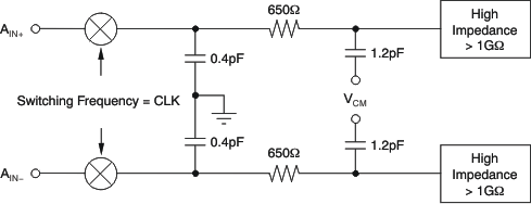
The input impedance of the analog input is dependent on the modulator clock frequency (fCLK), which is also the sampling frequency of the modulator. Figure 28 shows the basic input structure of one channel of the ADS1204. The relationship between the input impedance of the ADS1204 and the modulator clock frequency is shown in Equation 1:

The input impedance becomes a consideration in designs where the source impedance of the input signal is high. This high impedance may cause degradation in gain, linearity, and THD. The importance of this effect depends on the desired system performance. There are two restrictions on the analog input signals, CH x+ and CH x–. If the input voltage exceeds the range (GND – 0.3 V) to (VDD + 0.3 V), the input current must be limited to 10 mA because the input protection diodes on the front end of the converter will begin to turn on. In addition, the linearity and the noise performance of the device are ensured only when the differential analog voltage resides within ±2 V (with VREF as a midpoint); however, the FSR input voltage is ±2.5 V.
 Figure 28. Input Impedance of the ADS1204