SBAS301D October 2003 – February 2020 ADS1204
PRODUCTION DATA.
- 1 Features
- 2 Applications
- 3 Description
- 4 Revision History
- 5 Pin Configuration and Functions
- 6 Specifications
- 7 Detailed Description
- 8 Application and Implementation
- 9 Power Supply Recommendations
- 10Layout
- 11Device and Documentation Support
- 12Mechanical, Packaging, and Orderable Information
Package Options
Mechanical Data (Package|Pins)
- RHB|32
Thermal pad, mechanical data (Package|Pins)
- RHB|32
Orderable Information
7.1 Overview
The ADS1204 is a four-channel, second-order, CMOS device with four delta-sigma (ΔΣ) modulators, designed for medium- to high-resolution A/D signal conversions from dc to 39 kHz (filter response –3 dB) if an oversampling ratio (OSR) of 64 is chosen. The output of the converter (OUTX) provides a stream of digital ones and zeros. The time average of this serial output is proportional to the analog input voltage.
The modulator shifts the quantization noise to high frequencies. A low-pass digital filter should be used at the output of the ΔΣ modulator. The filter serves two functions. First, it filters out high-frequency noise. Second, the filter converts the 1-bit data stream at a high sampling rate into a higher-bit data word at a lower rate (decimation).
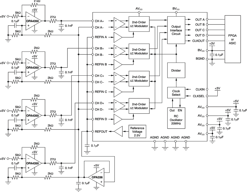
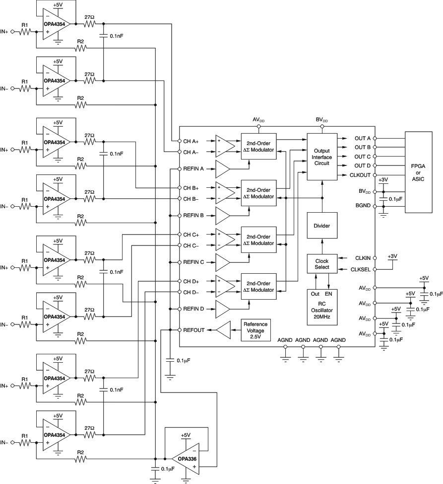
An application-specific integrated circuit (ASIC) or field-programmable gate array (FPGA) could be used to implement the digital filter. Figure 26 and Figure 27 illustrate typical application circuits with the ADS1204 connected to an FPGA.
The overall performance (that is, speed and accuracy) depends on the selection of an appropriate OSR and filter type. A higher OSR produces greater output accuracy while operating at a lower refresh rate. Alternatively, a lower OSR produces lower output accuracy, but operates at a higher refresh rate. This system allows flexibility with the digital filter design and is capable of A/D conversion results that have a dynamic range exceeding 100 dB with an OSR equal to 256.
 Figure 26. Single-Ended Connection Diagram for the ADS1204 ΔΣ Modulator
  Figure 27. Differential Connection Diagram for the ADS1204 ΔΣ Modulator