SBAS350H June 2005 – June 2025 ADS1232 , ADS1234
PRODUCTION DATA
- 1
- 1 Features
- 2 Applications
- 3 Description
- 4 Pin Configuration and Functions
- 5 Specifications
- 6 Parameter Measurement Information
-
7 Detailed Description
- 7.1 Overview
- 7.2 Functional Block Diagram
- 7.3
Feature Description
- 7.3.1 Analog Inputs (AINPX, AINNX)
- 7.3.2 Temperature Sensor (ADS1232 Only)
- 7.3.3 Low-Noise PGA
- 7.3.4 Voltage Reference Inputs (REFP, REFN)
- 7.3.5 Clock Sources
- 7.3.6 Digital Filter Frequency Response
- 7.3.7 Settling Time
- 7.3.8 Data Rate
- 7.3.9 Data Format
- 7.3.10 Data Ready and Data Output (DRDY/DOUT)
- 7.3.11 Serial Clock Input (SCLK)
- 7.3.12 Data Retrieval
- 7.4 Device Functional Modes
- 8 Application and Implementation
- 9 Device and Documentation Support
- 10Revision History
- 11Mechanical, Packaging, and Orderable Information
Package Options
Mechanical Data (Package|Pins)
- PW|24
Thermal pad, mechanical data (Package|Pins)
Orderable Information
8.2.3 Application Curves
To evaluate the ADC's noise performance, four fixed-value, 1-kΩ low-drift precision resistors are connected in a bridge arrangement to simulate a bridge sensor. The simulator provides the same thermal noise generated by a physical bridge. One of the four bridge resistors is modified to 1.008 kΩ in order to provide a 10-mV output signal. The 10-mV signal is typical of a 2-mV/V load cell using 5-V excitation.
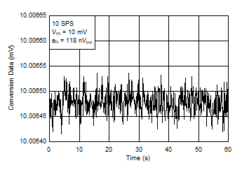
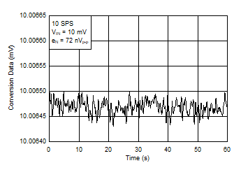
Figure 8-2 shows the ADC performance with data taken over a 60-second period. The 60-second period reveals true ADC peak-to-peak noise performance. Figure 8-3 shows the same conversion data processed by an external moving average filter (average x4). The noise-free resolution of the ADC is approximately 85,000 counts. Over the same 60-second period, the moving average filter improves noise-free resolution to 135,000 counts. The noise-free resolution (bits) corresponding to unfiltered and filtered data are 16.3 bits and 17.1 bits. See Equation 2 to calculate noise-free resolution in bits. In order to evaluate the actual noise-free resolution of the system, the 10-mV signal is used in the calculation, rather than the full input range of the ADC (39 mV = VREF / 128),
As shown in the noise plots, the moving average filter reduces noise by approximately one-half. As a consequence of the post filter operation, the input step settling time increases from 500 ms to 900 ms (500 ms because of the ADC settling response time, 400 ms because of the post-averaging filter).

