SBAS350G June 2005 – January 2021 ADS1232 , ADS1234
PRODUCTION DATA
- 1 Features
- 2 Applications
- 3 Description
- 4 Revision History
- 5 Pin Configuration and Functions
- 6 Specifications
- 7 Parameter Measurement Information
-
8 Detailed Description
- 8.1 Overview
- 8.2 Functional Block Diagram
- 8.3
Feature Description
- 8.3.1 Analog Inputs (AINPX, AINNX)
- 8.3.2 Temperature Sensor (ADS1232 Only)
- 8.3.3 Low-Noise PGA
- 8.3.4 Voltage Reference Inputs (REFP, REFN)
- 8.3.5 Clock Sources
- 8.3.6 Digital Filter Frequency Response
- 8.3.7 Settling Time
- 8.3.8 Data Rate
- 8.3.9 Data Format
- 8.3.10 Data Ready and Data Output (DRDY/DOUT)
- 8.3.11 Serial Clock Input (SCLK)
- 8.3.12 Data Retrieval
- 8.4 Device Functional Modes
- 9 Application and Implementation
- 10Power Supply Recommendations
- 11Layout
- 12Device and Documentation Support
- 13Mechanical, Packaging, and Orderable Information
Package Options
Mechanical Data (Package|Pins)
- PW|24
Thermal pad, mechanical data (Package|Pins)
Orderable Information
9.2 Typical Application
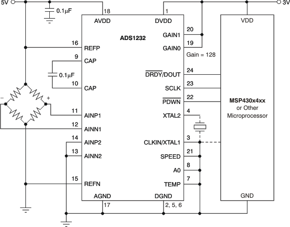
Figure 9-1 shows a circuit diagram of the ADS1232 as part of a weigh scale system. In this setup, the ADS1232 is configured to channel 1 input, gain = 128, and 10 SPS data rate. Gain = 128 is selected by tying the GAIN[1:0] pins to logic high (3 V in this example). Input channel 1 and data rate = 10 SPS are selected by tying input channel select pins A0 and TEMP to ground, and by tying the data rate select pin SPEED to ground. The unused channel 2 inputs are tied to ground.
The internal oscillator is selected by grounding the CLKIN/XTAL1 pin. The other clock options are 1) 4.9152-MHz crystal across the CLKIN/XTAL1 and XTAL2 pins, or 2) apply a clock to the CLKIN/XTAL1 pin (pin XTAL2 unconnected). The PWDN pin of the ADC is routed to the controller because this pin must be toggled after the ADC is powered. The bridge excitation voltage is connected to the ADC reference input pins (REFP, REFN). Not shown in Figure 9-1 are R-C input filters for the signal and reference inputs. If these filters are used, match the filter time constants to maintain cancellation of noise common to both signal and reference inputs.
 Figure 9-1 Weigh-Scale Application