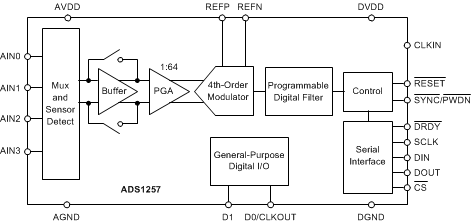
The ADS1257 is a low-noise, 30-kSPS, 24-bit, delta-sigma (ΔΣ) analog-to-digital converter (ADC) with an integrated multiplexer (mux), input buffer, and programmable gain amplifier (PGA) in a small 20-pin, 5-mm × 5-mm VQFN package. The combination of integration, high conversion rate, and 24-bit resolution together in a small package makes the device ideally suited for space-constrained applications.
The input multiplexer accepts either two differential or three single-ended input measurements. The sensor-break detection circuit verifies the input connection continuity to the ADC. The selectable input buffer greatly increases the input impedance, and in many cases, eliminates the need for external buffers. The buffer input voltage range includes AGND. The low-noise PGA provides gains from 1 to 64 to accommodate a wide range of inputs signals. The programmable digital filter optimizes ADC resolution (up to 23 bits noise-free) and conversion rates (up to 30 kSPS). The digital filter provides single-cycle settled conversions, and rejection of 50-Hz and 60-Hz interference signals.
The SPI-compatible serial interface operates with as little as three wires, simplifying connections to external controllers. Integrated calibration features support both self and system correction of offset and gain errors for all PGA gain settings. Two bidirectional digital I/Os pins control external circuits.
PART NUMBER | PACKAGE | BODY SIZE (NOM) |
---|---|---|
ADS1257 | VQFN (20) | 5.00 mm × 5.00 mm |
Changes from A Revision (October 2015) to B Revision
Changes from * Revision (September 2015) to A Revision
PIN | I/O | DESCRIPTION | |
---|---|---|---|
NO. | NAME | ||
1 | REFP | Analog input | Positive reference input |
2 | AIN0 | Analog input | Analog input 0; Leave unconnected or connect to AVDD if not used(4) |
3 | AIN1 | Analog input | Analog input 1; Leave unconnected or connect to AVDD if not used(4) |
4 | AIN2 | Analog input | Analog input 2; Leave unconnected or connect to AVDD if not used(4) |
5 | AIN3 | Analog input | Analog input 3; Leave unconnected or connect to AVDD if not used(4) |
6 | SYNC/PWDN | Digital input(1)(2) | Synchronization or power-down input, active low; Connect to DVDD if not used(4) |
7 | RESET | Digital input(1)(2) | Reset input, active low; Connect to DVDD if not used(4) |
8 | DVDD | Digital | Digital power supply; Connect decoupling capacitor to DGND |
9 | DGND | Digital | Digital ground |
10 | CLKIN | Digital input(2) | External clock input |
11 | CS | Digital input(1)(2) | Chip select, active low; Connect to DGND if not used |
12 | DRDY | Digital output | Data ready output; active low |
13 | DOUT | Digital output | Serial data output |
14 | DIN | Digital input(1)(2) | Serial data input |
15 | SCLK | Digital input(1)(2) | Serial clock input |
16 | D0/CLKOUT | Digital input/output(3) | General-purpose digital I/O 0 or clock output(4) |
17 | D1 | Digital input/output(3) | General-purpose digital I/O 1(4) |
18 | AVDD | Analog | Analog power supply; Connect decoupling capacitor to AGND |
19 | AGND | Analog | Analog ground |
20 | REFN | Analog input | Negative reference input |
Thermal Pad | — | Thermal power pad; Connect to AGND |
MIN | MAX | UNIT | ||
---|---|---|---|---|
Power-supply voltage | AVDD to AGND | –0.3 | 6.0 | V |
DVDD to DGND | –0.3 | 3.6 | ||
Analog input voltage | AINx, REFP, REFN | AGND – 0.3 | AVDD + 0.3 | V |
Digital input voltage | DIN, SCLK, CS, RESET, SYNC/PWDN, CLKIN | DGND – 0.3 | DGND + 6.0 | V |
D0/CLKOUT, D1 | DGND – 0.3 | DVDD + 0.3 | ||
Input current | Continuous, any pins except power-supply pins | –10 | 10 | mA |
Temperature | Operating ambient, TA | –40 | 105 | °C |
Junction, TJ | –40 | 150 | ||
Storage, Tstg | –60 | 150 |
VALUE | UNIT | |||
---|---|---|---|---|
V(ESD) | Electrostatic discharge | Human-body model (HBM), per ANSI/ESDA/JEDEC JS-001(1) | ±2000 | V |
Charged-device model (CDM), per JEDEC specification JESD22-C101(2) | ±500 |
MIN | NOM | MAX | UNIT | |||
---|---|---|---|---|---|---|
POWER SUPPLY | ||||||
Analog power supply | AVDD to AGND | 4.75 | 5 | 5.25 | V | |
Digital power supply | DVDD to DGND | 1.8 | 3.6 | V | ||
Analog-to-digital ground potential | AGND to DGND | –0.1 | 0 | 0.1 | V | |
ANALOG INPUTS | ||||||
VIN | Differential input voltage | VIN = V(AINP) – V(AINN) | –2 VREF / Gain | 2 VREF / Gain | V | |
V(AINx) | Absolute input voltage | Buffer off | AGND – 0.1 | AVDD + 0.1 | V | |
Buffer on | AGND | AVDD – 2.0 | ||||
VOLTAGE REFERENCE INPUTS | ||||||
VREF | Differential reference input voltage | VREF = V(REFP) – V(REFN) | 0.5 | 2.5 | 2.6 | V |
V(REFN) | Absolute negative reference input voltage | Buffer off | AGND – 0.1 | V(REFP) – 0.5 | V | |
Buffer on(1) | AGND | V(REFP) – 0.5 | ||||
V(REFP) | Absolute positive reference input voltage | Buffer off | V(REFN) + 0.5 | AVDD + 0.1 | V | |
Buffer on(1) | V(REFN) + 0.5 | AVDD – 2.0 | ||||
CLOCK SOURCE | ||||||
f(CLKIN) | Clock frequency | 0.1 | 7.68 | 10 | MHz | |
Duty cycle | 40% | 50% | 60% | |||
DIGITAL INPUTS | ||||||
Digital input voltage | DIN, SCLK, CS, RESET, SYNC/PWDN, CLKIN | DGND | DGND + 5.25 | V | ||
D0/CLKOUT, D1 | DGND | DVDD | ||||
TEMPERATURE | ||||||
TA | Operating ambient temperature | –40 | 85 | °C |
THERMAL METRIC(1) | ADS1257 | UNIT | |
---|---|---|---|
RGW (QFN) | |||
20 PINS | |||
RθJA | Junction-to-ambient thermal resistance | 32.0 | °C/W |
RθJC(top) | Junction-to-case (top) thermal resistance | 24.7 | °C/W |
RθJB | Junction-to-board thermal resistance | 10.4 | °C/W |
ψJT | Junction-to-top characterization parameter | 0.3 | °C/W |
ψJB | Junction-to-board characterization parameter | 10.4 | °C/W |
RθJC(bot) | Junction-to-case (bottom) thermal resistance | 1.6 | °C/W |
PARAMETER | TEST CONDITIONS | MIN | TYP | MAX | UNIT | |
---|---|---|---|---|---|---|
ANALOG INPUTS | ||||||
Gain | PGA gain | 1, 2, 4, 8, 16, 32, 64 | V/V | |||
Differential input impedance | Buffer off, gain = 1, 2, 4, 8, 16 | 150 / Gain | kΩ | |||
Buffer off, gain = 32, 64 | 4.7 | |||||
Buffer on, DR ≤ 50 SPS(1) | 80 | MΩ | ||||
SYSTEM PERFORMANCE | ||||||
Resolution | All data rates and PGA gain settings | 24 | Bit | |||
DR | Data rate | 2.5 | 30,000 | SPS | ||
INL | Integral nonlinearity | Differential input, gain = 1, buffer off | 3 | 10 | ppm | |
Differential input, gain = 64, buffer off | 7 | |||||
VIO | Input offset voltage | After calibration | On the level of the noise | |||
Offset drift | Gain = 1 | 100 | nV/°C | |||
Gain = 64 | 4 | |||||
Gain error | After calibration, gain = 1, buffer on | ±0.005% | ||||
After calibration, gain = 64, buffer on | ±0.03% | |||||
Gain drift | Gain = 1 | 0.8 | ppm/°C | |||
Gain = 64 | 0.8 | |||||
CMRR | Common-mode rejection ratio | fCM = 60 Hz, DR = 30 kSPS(2) | 95 | 110 | dB | |
PSRR | Power-supply rejection ratio | Analog, ±5% Δ in AVDD | 60 | 70 | dB | |
Digital, ±10% Δ in DVDD | 100 | dB | ||||
VOLTAGE REFERENCE INPUTS | ||||||
Reference input impedance | 18.5 | kΩ | ||||
SENSOR DETECT CURRENT SOURCES | ||||||
Current settings | 0.5, 2, 10 | µA | ||||
DIGITAL INPUTS/OUTPUTS | ||||||
VIH | High-level input voltage | DIN, SCLK, CLKIN, SYNC/PWDN, CS, RESET | 0.8 DVDD | 5.25 | V | |
D0/CLKOUT, D1 | 0.8 DVDD | DVDD | V | |||
VIL | Low-level input voltage | DGND | 0.2 DVDD | |||
VOH | High-level output voltage | IOH = 4 mA | 0.8 DVDD | V | ||
VOL | Low-level output voltage | IOL = 4 mA | 0.2 DVDD | V | ||
Input hysteresis | 0.5 | V | ||||
Input leakage | 0 < digital input voltage < DVDD | –10 | 10 | µA | ||
POWER SUPPLY | ||||||
IAVDD | Analog supply current | Power-down mode | 5 | µA | ||
Standby mode | 20 | µA | ||||
Normal mode, gain = 1, buffer off | 7 | 10 | mA | |||
Normal mode, gain = 64, buffer off | 16 | 24 | mA | |||
Normal mode, gain = 1, buffer on | 13 | 19 | mA | |||
Normal mode, gain = 64, buffer on | 36 | 50 | mA | |||
IDVDD | Digital supply current | Power-down mode | 5 | µA | ||
Standby mode, CLKOUT off, DVDD = 3.3 V | 95 | µA | ||||
Normal mode, CLKOUT off, DVDD = 3.3 V | 0.9 | 2 | mA | |||
PD | Power dissipation | Normal mode, gain = 1, buffer off, DVDD = 3.3 V | 38 | 57 | mW | |
Standby mode, DVDD = 3.3 V | 0.4 |
MIN | MAX | UNIT | |||
---|---|---|---|---|---|
t1 | SCLK period | 4 | t(CLKIN)(1) | ||
10 | t(DATA)(2) | ||||
t2H | Pulse duration, SCLK high | 200 | ns | ||
9 | t(DATA) | ||||
t2L | Pulse duration, SCLK low | 200 | ns | ||
t3 | Delay time, CS falling edge to first SCLK rising edge(3) | 50 | ns | ||
t4 | Setup time, DIN valid before SCLK falling edge | 50 | ns | ||
t5 | Hold time, DIN valid after SCLK falling edge | 50 | ns | ||
t6 | Delay time, last SCLK falling edge for DIN to first SCLK rising edge for DOUT: RDATA, RDATAC, RREG Commands | 50 | t(CLKIN) | ||
t10 | Delay time, final SCLK falling edge to CS rising edge | 8 | t(CLKIN) | ||
t11 | Delay time, final SCLK falling edge of command to first SCLK rising edge of next command | RREG, WREG, RDATA | 4 | t(CLKIN) | |
RDATAC, SDATAC, SYNC | 24 | t(CLKIN) | |||
t11B | Pulse duration, CS high | 4 | t(CLKIN) |
PARAMETER | TEST CONDITIONS | MIN | TYP | MAX | UNIT | |
---|---|---|---|---|---|---|
t7 | Propagation delay time, SCLK rising edge to valid new DOUT |
DOUT load = 20 pF || 100 kΩ to DGND | 50 | ns | ||
t8 | Propagation delay time, SCLK rising edge to DOUT invalid |
0 | ns | |||
t9 | Propagation delay time, last SCLK falling edge to DOUT high impedance |
6 | 10 | t(CLKIN) | ||
t11C | Propagation delay time, CS rising edge to DOUT high impedance |
0 | 50 | ns |
MIN | MAX | UNIT | |||
---|---|---|---|---|---|
t16 | Pulse duration, RESET, SYNC/PWDN low | 4 | t(CLKIN)(1) | ||
t16B | Delay time, SYNC/PWDN rising edge to CLKIN rising edge | –25 | 25 | ns |
MIN | MAX | UNIT | |||
---|---|---|---|---|---|
t12 | Pulse duration, first high pulse | 300 | 500 | t(CLKIN)(1) | |
t13 | Pulse duration, low pulse | 5 | t(CLKIN) | ||
t14 | Pulse duration, second high pulse | 550 | 750 | t(CLKIN) | |
t15 | Pulse duration, third high pulse | 1050 | 1250 | t(CLKIN) |
MIN | MAX | UNIT | |||
---|---|---|---|---|---|
t17 | Pulse duration, conversion data invalid while updating | 16 | t(CLKIN)(1) |
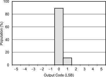
Gain = 1, 90 units from three production lots |
Gain = 1, data rate = 2.5 SPS, buffer = off, 256 readings |
Gain = 1, data rate = 1 kSPS, buffer = off, 4096 readings |
Gain = 1, data rate = 30 kSPS, buffer = off, 4096 readings |
Gain = 1 |
Gain = 1 |
Gain = 64, 90 units from three production lots |
Gain = 64, data rate = 2.5 SPS, buffer = off, 256 readings |
Gain = 64, data rate = 1 kSPS, buffer = off, 4096 readings |
Gain = 64, data rate = 30 kSPS, buffer = off, 4096 readings |
Gain = 1 |
The ADS1257 offers outstanding noise performance that can be optimized by adjusting the data rate or PGA gain setting. As the averaging is increased by reducing the data rate, the noise drops correspondingly. The PGA reduces the input-referred noise when measuring lower level signals. Table 1 through Table 4 summarize the typical noise performance with the inputs shorted externally.
In all four tables, the following conditions apply: TA = 25°C, AVDD = 5 V, DVDD = 1.8 V, VREF = 2.5 V, and f(CLKIN) = 7.68 MHz.
Table 1 and Table 3 show the root-mean-square (RMS) value of the input-referred noise. Table 2 and Table 4 show the effective number of bits of resolution (ENOB), using the noise data from Table 1 and Table 3 respectively. ENOB is defined as shown in Equation 1:
where
Table 2 and Table 4 also show the noise-free bits of resolution in parenthesis. Noise-free bits are calculated with the same formula as ENOB except the peak-to-peak noise values are used instead of RMS noise.
DATA RATE (SPS) |
PGA GAIN | ||||||
---|---|---|---|---|---|---|---|
1 | 2 | 4 | 8 | 16 | 32 | 64 | |
2.5 | 0.247 | 0.156 | 0.080 | 0.056 | 0.043 | 0.037 | 0.033 |
5 | 0.301 | 0.175 | 0.102 | 0.076 | 0.061 | 0.045 | 0.044 |
10 | 0.339 | 0.214 | 0.138 | 0.106 | 0.082 | 0.061 | 0.061 |
15 | 0.401 | 0.264 | 0.169 | 0.126 | 0.107 | 0.085 | 0.073 |
25 | 0.494 | 0.305 | 0.224 | 0.149 | 0.134 | 0.102 | 0.093 |
30 | 0.533 | 0.335 | 0.245 | 0.176 | 0.138 | 0.104 | 0.106 |
50 | 0.629 | 0.393 | 0.292 | 0.216 | 0.168 | 0.136 | 0.122 |
60 | 0.692 | 0.438 | 0.321 | 0.233 | 0.184 | 0.146 | 0.131 |
100 | 0.875 | 0.589 | 0.409 | 0.305 | 0.229 | 0.170 | 0.169 |
500 | 1.946 | 1.250 | 0.630 | 0.648 | 0.497 | 0.390 | 0.367 |
1000 | 2.931 | 1.891 | 1.325 | 1.070 | 0.689 | 0.512 | 0.486 |
2000 | 4.173 | 2.589 | 1.827 | 1.492 | 0.943 | 0.692 | 0.654 |
3750 | 5.394 | 3.460 | 2.376 | 1.865 | 1.224 | 0.912 | 0.906 |
7500 | 7.249 | 4.593 | 3.149 | 2.436 | 1.691 | 1.234 | 1.187 |
15,000 | 9.074 | 5.921 | 3.961 | 2.984 | 2.125 | 1.517 | 1.515 |
30,000 | 10.728 | 6.705 | 4.446 | 3.280 | 2.416 | 1.785 | 1.742 |
DATA RATE (SPS) |
PGA GAIN | |||||||||||||
---|---|---|---|---|---|---|---|---|---|---|---|---|---|---|
1(1) | 2 | 4 | 8 | 16 | 32 | 64 | ||||||||
2.5 | 24.5 | (22.3) | 24.9 | (22.6) | 24.9 | (22.1) | 24.4 | (21.7) | 23.8 | (21.3) | 23.0 | (20.8) | 22.2 | (19.7) |
5 | 24.2 | (21.6) | 24.8 | (22.4) | 24.5 | (21.9) | 24.0 | (21.3) | 23.3 | (20.7) | 22.7 | (20.3) | 21.8 | (19.3) |
10 | 24.1 | (21.6) | 24.5 | (22.0) | 24.1 | (21.6) | 23.5 | (21.0) | 22.9 | (20.4) | 22.3 | (19.9) | 21.3 | (18.9) |
15 | 23.8 | (21.3) | 24.2 | (21.7) | 23.8 | (21.3) | 23.2 | (20.7) | 22.5 | (20.1) | 21.8 | (19.3) | 21.0 | (18.7) |
25 | 23.5 | (21.0) | 24.0 | (21.4) | 23.4 | (21.1) | 23.0 | (20.5) | 22.2 | (19.7) | 21.5 | (19.2) | 20.7 | (18.5) |
30 | 23.4 | (21.1) | 23.8 | (21.3) | 23.3 | (20.8) | 22.8 | (20.4) | 22.1 | (19.8) | 21.5 | (19.0) | 20.5 | (18.1) |
50 | 23.2 | (20.6) | 23.6 | (21.1) | 23.0 | (20.4) | 22.5 | (19.9) | 21.8 | (19.4) | 21.1 | (18.8) | 20.3 | (17.9) |
60 | 23.0 | (20.6) | 23.4 | (20.9) | 22.9 | (20.5) | 22.4 | (19.8) | 21.7 | (19.3) | 21.0 | (18.8) | 20.2 | (17.8) |
100 | 22.7 | (20.2) | 23.0 | (20.7) | 22.5 | (20.2) | 22.0 | (19.6) | 21.4 | (19.1) | 20.8 | (18.5) | 19.8 | (17.4) |
500 | 21.6 | (19.4) | 21.9 | (19.6) | 21.5 | (19.1) | 20.9 | (18.6) | 20.3 | (18.0) | 19.6 | (17.3) | 18.7 | (16.3) |
1000 | 21.0 | (18.3) | 21.3 | (18.6) | 20.8 | (18.1) | 20.2 | (17.5) | 19.8 | (17.2) | 19.2 | (16.5) | 18.3 | (15.6) |
2000 | 20.5 | (17.8) | 20.9 | (18.1) | 20.4 | (17.8) | 19.7 | (17.0) | 19.3 | (16.6) | 18.8 | (16.1) | 17.9 | (15.3) |
3750 | 20.1 | (17.4) | 20.5 | (17.8) | 20.0 | (17.3) | 19.4 | (16.6) | 19.0 | (16.2) | 18.4 | (15.7) | 17.4 | (14.7) |
7500 | 19.7 | (17.0) | 20.1 | (17.3) | 19.6 | (16.9) | 19.0 | (16.2) | 18.5 | (15.8) | 17.9 | (15.3) | 17.0 | (14.4) |
15,000 | 19.3 | (16.6) | 19.7 | (17.0) | 19.3 | (16.5) | 18.7 | (15.9) | 18.2 | (15.5) | 17.7 | (14.9) | 16.7 | (13.9) |
30,000 | 19.1 | (16.4) | 19.5 | (16.7) | 19.1 | (16.4) | 18.5 | (15.9) | 18.0 | (15.4) | 17.4 | (14.6) | 16.5 | (13.8) |
DATA RATE (SPS) |
PGA GAIN | ||||||
---|---|---|---|---|---|---|---|
1 | 2 | 4 | 8 | 16 | 32 | 64 | |
2.5 | 0.247 | 0.149 | 0.097 | 0.058 | 0.036 | 0.031 | 0.027 |
5 | 0.275 | 0.176 | 0.109 | 0.07 | 0.046 | 0.039 | 0.038 |
10 | 0.338 | 0.201 | 0.129 | 0.084 | 0.063 | 0.048 | 0.047 |
15 | 0.401 | 0.221 | 0.15 | 0.109 | 0.07 | 0.063 | 0.057 |
25 | 0.485 | 0.279 | 0.177 | 0.136 | 0.093 | 0.076 | 0.076 |
30 | 0.559 | 0.315 | 0.202 | 0.142 | 0.107 | 0.093 | 0.082 |
50 | 0.644 | 0.39 | 0.238 | 0.187 | 0.129 | 0.108 | 0.103 |
60 | 0.688 | 0.417 | 0.281 | 0.204 | 0.134 | 0.109 | 0.111 |
100 | 0.815 | 0.53 | 0.36 | 0.233 | 0.169 | 0.123 | 0.122 |
500 | 1.957 | 1.148 | 0.772 | 0.531 | 0.375 | 0.276 | 0.259 |
1000 | 2.803 | 1.797 | 1.191 | 0.94 | 0.518 | 0.392 | 0.365 |
2000 | 4.025 | 2.444 | 1.615 | 1.31 | 0.7 | 0.526 | 0.461 |
3750 | 5.413 | 3.25 | 2.061 | 1.578 | 0.914 | 0.693 | 0.625 |
7500 | 7.017 | 4.143 | 2.722 | 1.998 | 1.241 | 0.914 | 0.857 |
15,000 | 8.862 | 5.432 | 3.378 | 2.411 | 1.569 | 1.149 | 1.051 |
30,000 | 10.341 | 6.137 | 3.873 | 2.775 | 1.805 | 1.313 | 1.211 |
DATA RATE (SPS) |
PGA GAIN | |||||||||||||
---|---|---|---|---|---|---|---|---|---|---|---|---|---|---|
1 | 2 | 4 | 8 | 16 | 32 | 64 | ||||||||
2.5 | 25.3 | (23.0) | 25.0 | (22.4) | 24.6 | (22.0) | 24.4 | (21.9) | 24.0 | (21.3) | 23.2 | (21.1) | 22.5 | (20.0) |
5 | 25.1 | (22.4) | 24.8 | (22.1) | 24.5 | (21.9) | 24.1 | (21.5) | 23.7 | (21.2) | 22.9 | (20.4) | 22.0 | (19.4) |
10 | 24.8 | (22.3) | 24.6 | (22.1) | 24.2 | (21.7) | 23.8 | (21.5) | 23.2 | (20.8) | 22.6 | (20.3) | 21.7 | (19.2) |
15 | 24.6 | (22.0) | 24.4 | (21.8) | 24.0 | (21.4) | 23.4 | (20.8) | 23.1 | (20.6) | 22.2 | (19.9) | 21.4 | (19.0) |
25 | 24.3 | (21.8) | 24.1 | (21.7) | 23.8 | (21.1) | 23.1 | (20.7) | 22.7 | (20.3) | 22.0 | (19.5) | 21.0 | (18.6) |
30 | 24.1 | (21.6) | 23.9 | (21.4) | 23.6 | (21.1) | 23.1 | (20.4) | 22.5 | (20.0) | 21.7 | (16.4) | 20.9 | (18.5) |
50 | 23.9 | (21.3) | 23.6 | (21.3) | 23.3 | (20.7) | 22.7 | (20.1) | 22.2 | (19.8) | 21.5 | (19.1) | 20.5 | (18.2) |
60 | 23.8 | (21.2) | 23.5 | (21.0) | 23.1 | (20.6) | 22.5 | (20.0) | 22.1 | (19.8) | 21.5 | (19.1) | 20.4 | (18.1) |
100 | 23.5 | (21.1) | 23.2 | (20.5) | 22.7 | (20.3) | 22.4 | (19.9) | 21.8 | (19.5) | 21.3 | (19.0) | 20.3 | (17.9) |
500 | 22.3 | (20.0) | 22.1 | (19.7) | 21.6 | (19.3) | 21.2 | (18.9) | 20.7 | (18.3) | 20.1 | (17.8) | 19.2 | (16.9) |
1000 | 21.8 | (19.0) | 21.4 | (18.7) | 21.0 | (18.4) | 20.3 | (17.7) | 20.2 | (17.5) | 19.6 | (16.9) | 18.7 | (15.9) |
2000 | 21.2 | (18.5) | 21.0 | (18.3) | 20.6 | (17.9) | 19.9 | (17.4) | 19.8 | (17.0) | 19.2 | (16.4) | 18.4 | (15.6) |
3750 | 20.8 | (18.1) | 20.6 | (17.8) | 20.2 | (17.5) | 19.6 | (17.0) | 19.4 | (16.7) | 18.8 | (16.1) | 17.9 | (15.2) |
7500 | 20.4 | (17.7) | 20.2 | (17.6) | 19.8 | (17.0) | 19.3 | (16.6) | 18.9 | (16.2) | 18.4 | (15.7) | 17.5 | (14.8) |
15,000 | 20.1 | (17.4) | 19.8 | (17.1) | 19.5 | (16.8) | 19.0 | (16.3) | 18.6 | (15.9) | 18.1 | (15.3) | 17.2 | (14.4) |
30,000 | 19.9 | (17.1) | 19.6 | (17.0) | 19.3 | (16.6) | 18.8 | (16.0) | 18.4 | (15.6) | 17.9 | (15.0) | 17.0 | (14.3) |
The ADS1257 is a very low-noise ADC that supports four analog inputs and offers two general-purpose digital I/Os. The Functional Block Diagram shows a block diagram of the ADS1257. The input multiplexer selects the ADC input pin connection. Selectable current sources within the input multiplexer check for open- or short-circuit conditions on the external sensor. A selectable input buffer greatly reduces the input circuitry loading by providing up to 80 MΩ of impedance. A low-noise PGA provides gains of 1 V/V, 2 V/V, 4 V/V, 8 V/V, 16 V/V, 32 V/V, or 64 V/V. The ADS1257 is comprised of a fourth-order, delta-sigma modulator followed by a programmable digital filter.
The modulator measures the amplified differential input signal, VIN · Gain = (V(AINP) – V(AINN)) · Gain, against the differential reference, VREF = V(REFP) − V(REFN). The ADC requires an external reference voltage to operate. The differential reference is scaled internally by a factor of two so that the full-scale input range is ±2 · VREF / Gain.
The digital filter receives the modulator signal and provides a low-noise digital output. The data rate of the filter is programmable from 2.5 SPS to 30 kSPS, and allows tradeoffs between resolution and speed.
Communication is over an SPI-compatible serial interface with a set of commands providing control of the ADS1257. The configuration registers store the various settings for the input multiplexer, sensor-detect current sources, input buffer enable, PGA gain setting, output data rate, and more. The ADC requires an external clock source to operate. General-purpose digital I/Os provide static read and write control of up to two pins. The D0 pin is also used to supply a programmable clock output.
Figure 23 shows a simplified diagram of the input multiplexer. Select any pin as the positive input (AINP) and any pin as the negative input (AINN). Pin selection is controlled by the MUX register.
The ADS1257 offers four analog inputs that can be configured as two independent differential inputs, three single-ended inputs, or a combination of differential and single-ended inputs.
In general, there are no restrictions on input-pin selection. However, follow these recommendations for optimal performance:
ESD diodes protect the analog inputs. To keep these diodes from turning on, voltages on the input pins must not go below AGND by more than 100 mV, and likewise, must not exceed AVDD by more than 100 mV: −100 mV < (V(AINx)) < AVDD + 100 mV.
To increase the input impedance presented by the ADS1257, enable the low-drift, chopper-stabilized buffer using the BUFEN bit in the STATUS register. As shown in Figure 24, the input impedance with the buffer enabled is modeled by a resistor. Table 5 lists the values of Zeff for the different data-rate settings. The input impedance scales inversely with the frequency of CLKIN. For example, if f(CLKIN) is reduced by half to 3.84 MHz, Zeff for a data-rate setting of 50 SPS (actual data rate of 25 SPS) doubles from 80 MΩ to 160 MΩ.s
DATA RATE (SPS) |
Zeff (MΩ) |
---|---|
≤ 50 | 80 |
60 | 40 |
100 | 40 |
500 | 40 |
1,000 | 20 |
2,000 | 10 |
3,750 | 10 |
7,500 | 10 |
15,000 | 10 |
30,000 | 10 |
NOTE
With the buffer enabled, the voltage on the analog inputs with respect to ground (listed in the Recommended Operating Conditions as Absolute Input Voltage) must remain between AGND and AVDD − 2.0 V. Exceeding this range reduces performance; in particular, the linearity of the ADS1257. This same voltage range, AGND to AVDD − 2.0 V, applies to the reference inputs when performing a self-gain calibration with the buffer enabled.
The ADS1257 is a very high resolution converter. To further complement converter performance, the low-noise PGA increases the ADC resolution when measuring smaller input signals. For the best resolution, set the PGA to the highest possible gain setting. The gain setting depends on the largest input signal to be measured. The ADS1257 full-scale input voltage equals ±2 · VREF / Gain. Table 6 shows the full-scale input voltage for the different PGA gain settings for VREF = 2.5 V. For example, if the largest signal to be measured is 1.0 V, the optimum PGA gain setting is 4 V/V, producing a full-scale input voltage of 4 V with no ADC overrange.
PGA GAIN SETTING | FULL-SCALE INPUT VOLTAGE VIN (1)
(VREF = 2.5 V) |
---|---|
1 | ±5 V |
2 | ±2.5 V |
4 | ±1.25 V |
8 | ±0.625 V |
16 | ±312.5 mV |
32 | ±156.25 mV |
64 | ±78.125 mV |
The PGA is controlled by the ADCON register. Recalibrate the ADC after changing the PGA gain setting. The time required for self-calibration depends on the PGA gain setting; see the Calibration section for more details. The analog current and input impedance (when the buffer is disabled) vary as a function of the PGA gain setting.
The ADS1257 modulator measures the input signal using internal capacitors that are continuously charged and discharged. Figure 25 shows a simplified schematic of the ADS1257 input circuitry with the input buffer disabled. The on and off timing of the S1 and S2 switches are shown in Figure 26. The S1 switch closes during the input sampling phase. With S1 closed, CA1 charges to V(AINP), CA2 charges to V(AINN), and CB charges to
(V(AINP) – V(AINN)). For the discharge phase, S1 opens first and then S2 closes. CA1 and CA2 discharge to approximately AVDD / 2 and CB discharges to 0 V. This two-phase sample and discharge cycle repeats with a period of tSAMPLE. This time is a function of the PGA gain setting as shown in Table 7 along with the values of capacitors CA1 = CA2 = CA and CB.
PGA GAIN SETTING | tSAMPLE(1) | CA | CB |
---|---|---|---|
1 | f(CLKIN) / 4 (521 ns) | 2.1 pF | 2.4 pF |
2 | f(CLKIN) / 4 (521 ns) | 4.2 pF | 4.9 pF |
4 | f(CLKIN) / 4 (521 ns) | 8.3 pF | 9.7 pF |
8 | f(CLKIN) / 4 (521 ns) | 17 pF | 19 pF |
16 | f(CLKIN) / 4 (521 ns) | 33 pF | 39 pF |
32 | f(CLKIN) / 2 (260 ns) | 33 pF | 39 pF |
64 | f(CLKIN) / 2 (260 ns) | 33 pF | 39 pF |
The charging of the input capacitors draws a transient current from the sensor driving the ADS1257 inputs. The average value of this current is used to calculate an effective impedance Zeff, where Zeff = VIN / IAVERAGE. Figure 27 shows the input circuitry with the capacitors and switches of Figure 25 replaced by their effective impedances. These impedances scale inversely with the CLKIN frequency. For example, if f(CLKIN) is reduced by a factor of two, the impedances double. The impedance also changes with the PGA gain setting. Table 8 lists the effective impedances with the buffer off for f(CLKIN) = 7.68 MHz.
PGA GAIN SETTING | ZeffA
(kΩ) |
ZeffB
(kΩ) |
---|---|---|
1 | 260 | 220 |
2 | 130 | 110 |
4 | 65 | 55 |
8 | 33 | 28 |
16 | 16 | 14 |
32 | 8 | 7 |
64 | 8 | 7 |
The ADC requires a reference voltage for operation. The reference voltage for the ADS1257 is the differential voltage between REFP and REFN: VREF = V(REFP) − V(REFN). The reference inputs use a structure similar to that of the analog inputs with the circuitry on the reference inputs of Figure 28. The load presented by the switched capacitor is modeled with an effective impedance (Zeff) of 18.5 kΩ for f(CLKIN) = 7.68 MHz. The temperature coefficient of the effective impedance of the voltage reference inputs is approximately 35 ppm/°C.
ESD diodes protect the reference inputs. To keep these diodes from turning on, the voltages on the reference pins must not go below AGND by more than 100 mV, and must not exceed AVDD by 100 mV:
AGND − 100 mV < (V(REFP) or V(REFN)) < AVDD + 100 mV
During self gain calibration, all the switches in the input multiplexer are opened, REFN is internally connected to AINN, and REFP is connected to AINP. The input buffer can be disabled or enabled during calibration. When the buffer is disabled, the reference pins drive the circuitry shown in Figure 25 during self gain calibration, resulting in increased loading. To prevent this additional loading from introducing gain errors, the circuitry driving the reference pins must have adequate drive capability. When the buffer is enabled, the loading on the reference pins is much less. However, the buffer limits the allowable voltage range on REFP and REFN during self- or self gain calibration because the reference pins must remain within the specified input range of the buffer in order to establish proper gain calibration.
A high-quality reference voltage capable of driving the switched capacitor load presented by the ADS1257 is essential for achieving the best performance. Noise and drift on the reference degrade overall system performance. Take special care with the circuitry generating the reference voltages and their layout when operating with low-noise settings (that is, with low data rates) in order to prevent the voltage reference from limiting performance.
See the External Reference section for more details.
The master clock for the ADS1257 must be applied to the CLKIN pin. Keep the external clock signal clean and free of overshoot. Overshoot and glitches on the clock degrade overall performance. See the Recommended Operating Conditions section for the recommended master clock frequency range. Some of the timing requirements, as well as the output data rate, scale directly with the CLKIN frequency.
Use the clock output pin (D0/CLKOUT) to clock another device, such as another ADS1257 or a microcontroller. This clock operates at frequencies of f(CLKIN), f(CLKIN) / 2, or f(CLKIN) / 4 and is configured by setting the CLK[1:0] bits in the ADCON register. If the output clock is enabled while driving an external load, the digital power consumption increases. Standby mode does not affect the clock output status. That is, if standby is enabled, the clock output continues to run during standby mode. If not needed, disable the clock output function by writing to the CLK bits in the ADCON register after power-up or reset.
The ADS1257 offers two pins dedicated for general-purpose digital I/Os. All of the digital I/O pins can be individually configured as either inputs or outputs through the IO register. The DIR bits of the IO register define whether each pin is an input or output, and the DIO bits control the status of the pins. Reading back the DIO bits shows the state of the digital I/O pins; that is, if configured as inputs or outputs by the DIR bits. When digital I/O pins are configured as inputs, the DIO bits are used to read the state of these pins. When configured as outputs, writing to the DIO bits sets the output value.
During standby and power-down modes, the GPIOs remain active. If configured as outputs, the GPIOs continue to drive the pins. If configured as inputs, the GPIOs must be driven (not left floating) to prevent excess power dissipation.
After power-up or reset, the D1 pin defaults to an input and the D0/CLKOUT pin defaults to the clock output. The CLK[1:0] bits that control the clock output on D0/CLKOUT are only reset after power-up or RESET pin toggle. If the digital I/O pins are not used, either leave them as inputs tied to ground, or configure them as outputs and leave them floating to avoid excess power dissipation.
The sensor detect current sources (SDCS) provide a means to verify the integrity of the external sensor connected to the ADS1257. When enabled, the SDCS supply a current (ISDC) of approximately 0.5 μA, 2 μA, or 10 μA to the sensor through the input multiplexer. The SDCS bits in the ADCON register enable the SDCS and set the value of ISDC.
When the SDCS are enabled, the ADS1257 automatically turns on the analog input buffer, regardless of the BUFEN bit setting, in order to prevent the input circuitry from loading the SDCS. AINP must stay below 3 V to be within the absolute input range of the buffer. To help meet this condition, a 3-V clamp starts sinking current from AINP to AGND if AINP exceeds 3 V. Note that this clamp is activated only when the SDCS are enabled.
Figure 29 shows a simplified diagram of the ADS1257 input structure with the external sensor modeled as resistance RSENS between two input pins. When enabled, the SDCS source ISDC to the input pin connected to AINP, and sink ISDC from the input pin connected to AINN. The two 25-Ω series resistors, RMUX, model the ADS1257 internal multiplexer switch on-resistances. The signal measured with the SDCS enabled equals the total IR drop: ISDC × (2RMUX + RSENS). When the sensor is a direct short (that is, RSENS = 0 Ω), there is still a small signal measured by the ADS1257 when the SDCS are enabled: ISDC · 2RMUX.
The programmable low-pass digital filter receives the modulator output and produces a high-resolution digital output. By adjusting the amount of filtering, tradeoffs can be made between resolution and data rate: filter more for higher resolution, or filter less for higher data rate. The filter is comprised of two sections, a fixed filter followed by a programmable filter. Figure 30 shows the block diagram of the analog modulator and digital filter. Data are supplied to the filter from the analog modulator at a rate of f(MOD) = f(CLKIN) / 4. The fixed filter is a fifth-order sinc filter with a decimation value of 64 that outputs data at a rate of f(CLKIN) / 256. The second stage of the filter is a programmable averager (first-order sinc filter) with the number of averages set by the DRATE register. The data rate is a function of the number of averages (Num_Ave) and is given by Equation 2.
Table 9 shows the averaging and corresponding data rate for each of the 16 valid DRATE register settings when f(CLKIN) = 7.68 MHz. The data rate scales directly with the CLKIN frequency. For example, reducing f(CLKIN) from 7.68 MHz to 3.84 MHz reduces the data rate for DR[7:0] = 1111 0000 from 30,000 SPS to 15,000 SPS.
DRATE[7:0] | NUMBER OF AVERAGES FOR PROGRAMMABLE FILTER (Num_Ave) |
DATA RATE(1)
(SPS) |
---|---|---|
0000 0011 (03h) | 12,000 | 2.5 |
0001 0011 (13h) | 6000 | 5 |
0010 0011 (23h) | 3000 | 10 |
0011 0011 (33h) | 2000 | 15 |
0100 0011 (43h) | 1200 | 25 |
0101 0011 (53h) | 1000 | 30 |
0110 0011 (63h) | 600 | 50 |
0111 0010 (72h) | 500 | 60 |
1000 0010 (82h) | 300 | 100 |
1001 0010 (92h) | 60 | 500 |
1010 0001 (A1h) | 30 | 1000 |
1011 0000 (B0h) | 15 | 2000 |
1100 0000 (C0h) | 8 | 3750 |
1101 0000 (D0h) | 4 | 7500 |
1110 0000 (E0h) | 2 | 15,000 |
1111 0000 (F0h) | 1 (averager bypassed) | 30,000 |
The low-pass digital filter sets the overall frequency response for the ADS1257. The filter response is the product of the responses of the fixed and programmable filter sections, and is given by Equation 3:
The digital filter attenuates noise on the modulator output, including noise from within the ADS1257 and external noise present on the ADS1257 input signal. Adjusting the filtering by changing the number of averages used in the programmable filter changes the filter bandwidth. With a higher number of averages, bandwidth is reduced, and more noise is attenuated.
The low-pass filter has notches (or zeros) at the data output rate and multiples thereof. At these frequencies, the filter has zero gain. This feature is useful when trying to reject a particular interference signal. For example, to reduce 60-Hz (and harmonic) noise coupling, set the data rate equal to 2.5 SPS, 5 SPS, 10 SPS, 15 SPS, 30 SPS, or 60 SPS. To help illustrate the filter characteristics, Figure 31 and Figure 32 show the responses at the data-rate extremes of 30 kSPS and 2.5 SPS, respectively.
Table 10 summarizes the first-notch frequency and −3-dB bandwidth for the different data-rate settings.
DATA RATE (SPS) |
FIRST NOTCH (Hz) |
-3 dB BANDWIDTH (Hz) |
---|---|---|
2.5 | 2.5 | 1.1 |
5 | 5 | 2.21 |
10 | 10 | 4.42 |
15 | 15 | 6.63 |
25 | 25 | 11.1 |
30 | 30 | 13.3 |
50 | 50 | 22.1 |
60 | 60 | 26.5 |
100 | 100 | 44.2 |
500 | 500 | 221 |
1000 | 1000 | 441 |
2000 | 2000 | 878 |
3750 | 3750 | 1615 |
7500 | 7500 | 3003 |
15,000 | 15,000 | 4807 |
30,000 | 30,000 | 6106 |
The digital filter low-pass characteristic repeats at multiples of the modulator rate of f(MOD) = f(CLKIN) / 4. Figure 33 and Figure 34 show the responses plotted out to 7.68 MHz at the data-rate extremes of 30 kSPS and 2.5 SPS. Notice how the responses near dc, 1.92 MHz, 3.84 MHz, 5.76 MHz, and 7.68 MHz are the same. The digital filter attenuates high-frequency noise on the ADS1257 inputs, except for frequencies where the filter response repeats. External filtering is required to remove high-frequency input noise near these pass-band regions. See the Analog Input Filtering section for more details.
As a result of the proximity of the signal wires to industrial motors and conductors in some applications, coupling of 50-Hz and 60-Hz power-line frequencies can occur. Coupled noise can interfere with the signal voltage leading to inaccurate or unstable conversions. The digital filter rejects power-line interference for data rates of 60 SPS and less. Program the filter to tradeoff data rate and conversion latency versus the desired level of line-cycle rejection. Table 11 summarizes the 50-Hz and 60-Hz line-cycle rejection based on 2% tolerance of power-line frequency to ADC clock frequency.
DATA RATE (SPS) |
MINIMUM DIGITAL-FILTER MAGNITUDE (dB) | |
---|---|---|
50 Hz ±2% | 60 Hz ±2% | |
2.5 | –36.2 | –37.4 |
5 | –34.4 | –34.6 |
10 | –33.9 | –34.0 |
15 | — | –33.9 |
25 | –33.8 | — |
30 | — | –33.8 |
50 | –33.8 | — |
60 | — | –33.8 |
The ADS1257 features a digital filter optimized for fast settling. The Conversion Control and Synchronization section describes the settling time of the ADS1257 for various modes of operation.
All configuration registers are initialized to default states at power-up. Self-calibration is then performed automatically. For best performance, issue an additional self-calibration with the SELFCAL command or reset the device after the power supplies and voltage reference have settled to their final values.
NOTE
A reset is required after power-up to avoid invalid device operation.
Three methods are used to reset the ADS1257: the RESET pin, the RESET command, and a special SCLK reset pattern.
After the device resets, the configuration registers are initialized to their default state, except for the CLK[1:0] bits in the ADCON register that control the D0/CLKOUT pin. The CLK[1:0] bits are only initialized to their default state when reset is performed using the RESET pin. Reset also exits from the read-data continuous mode.
After a reset, the device self-calibrates, regardless of the reset method or the state of the ACAL bit before the reset.
Standby mode shuts down all of the analog circuitry and most of the digital features. To enter standby mode, issue the STANDBY command. To exit standby mode, issue the WAKEUP command. DRDY stays high after exiting standby mode until valid data are ready.
Use standby mode to perform single-shot conversions; see the Settling Time Using Single-Shot Mode section for more information.
If configured as a clock output, the clock signal on the D0/CLKOUT pin continues to run during standby mode.
Hold the SYNC/PWDN pin low for 20 DRDY cycles to activate power-down mode. During power-down mode, all circuitry is disabled including the clock output.
To exit power-down mode, take the SYNC/PWDN pin high. After exiting from power-down mode, 8192 · t(CLKIN) cycles are required before conversions begin.
Device synchronization is available to control the beginning of the analog-to-digital conversion with an external event, and also to improve settling time after a multiplexer change. Two methods are provided to perform synchronization, the SYNC/PWDN pin or the SYNC command:
After a synchronization operation, either with the SYNC/PWDN pin or the SYNC command, DRDY stays high until valid data are ready.
The settling time (that is, the time required for a step change on the analog inputs to propagate through the filter) for the different data rates is shown in Table 12 and Figure 35. The following sections highlight the single-cycle settling ability of the filter, and show various ways to control the conversion process.
DATA RATE (SPS) |
SETTLING TIME (t18) (ms) |
---|---|
2.5 | 400.18 |
5 | 200.18 |
10 | 100.18 |
15 | 66.84 |
25 | 40.18 |
30 | 33.51 |
50 | 20.18 |
60 | 16.84 |
100 | 10.18 |
500 | 2.18 |
1000 | 1.18 |
2000 | 0.68 |
3750 | 0.44 |
7500 | 0.31 |
15,000 | 0.25 |
30,000 | 0.21 |
The SYNC/PWDN pin and SYNC command allow direct control of conversion timing. Issue a SYNC command or toggle the SYNC/PWDN pin after changing the analog inputs to restart conversions (see the Conversion Control and Synchronization section for more information). The conversion begins when SYNC/PWDN is taken high, thus stopping the current conversion, and restarting the digital filter. As soon as SYNC/PWDN goes low, the DRDY output goes high and remains high during the conversion. DRDY goes low after the settling time (t18, listed for each data rate in Table 12), indicating that data are available. There is no need to ignore or discard data after synchronization. Figure 35 shows the data retrieval sequence following synchronization.
To reduce power consumption in the ADS1257, perform single-shot conversions using the STANDBY command. The sequence for the STANDBY command is shown in Figure 36. Issue the WAKEUP command from standby mode to begin a single-shot conversion. When using single-shot mode, an additional delay is required for the modulator to power up and settle. This delay may require up to 64 modulator clocks (64 · 4 · t(CKLIN)), or 33.3 μs for a 7.68-MHz master clock. Following the settling time (t18 + 256 · t(CLKIN)), DRDY goes low, indicating that the conversion is complete and data can be read using the RDATA command. The ADS1257 settles in a single cycle; there is no need to ignore or discard data. Following the data read cycle, issue another STANDBY command to reduce power consumption. When ready for the next measurement, repeat the cycle starting with another WAKEUP command.
The most efficient way to cycle through the inputs is to change the multiplexer setting immediately after DRDY goes low. Changing the multiplexer before reading the data allows the ADS1257 to start sampling the new input channel sooner. Figure 37 demonstrates efficient input cycling. There is no need to ignore or discard data while cycling through the channels of the input multiplexer because the ADS1257 data are fully settled when DRDY goes low.
Step 1: When DRDY goes low (indicating that data are ready for retrieval), update the MUX register using the WREG command. For example, setting MUX to 23h selects AINP = AIN2, AINN = AIN3.
Step 2: Restart the conversion process by issuing a SYNC command followed by a WAKEUP command. Follow timing specification t11 between commands.
Step 3: Read the data from the previous conversion using the RDATA command. Repeat this process when DRDY goes low.
Table 13 gives the effective overall throughput (1 / t19) when cycling the input multiplexer. The values for throughput (1 / t19) assume the multiplexer is changed with a 3-byte WREG command and f(SCLK) = f(CLKIN) / 4.
DATA RATE (SPS) |
CYCLING THROUGHPUT (1 / t19) (Hz) |
---|---|
2.5 | 2.5 |
5 | 5 |
10 | 10 |
15 | 15 |
25 | 25 |
30 | 30 |
50 | 50 |
60 | 59 |
100 | 98 |
500 | 456 |
1000 | 837 |
2000 | 1438 |
3750 | 2165 |
7500 | 3043 |
15,000 | 3817 |
30,000 | 4374 |
After a synchronization, input multiplexer change, or wakeup from standby mode, the ADS1257 continuously converts the analog input. The conversions coincide with the falling edge of DRDY. While continuously converting, the settling time is given by a number of DRDY periods, as shown in Table 14. The DRDY period equals the inverse of the selected data rate.
DATA RATE (SPS) |
SETTLING TIME (DRDY PERIODS) |
---|---|
2.5 | 1 |
5 | 1 |
10 | 1 |
15 | 1 |
25 | 1 |
30 | 1 |
50 | 1 |
60 | 1 |
100 | 1 |
500 | 1 |
1000 | 1 |
2000 | 1 |
3750 | 1 |
7500 | 2 |
15,000 | 3 |
30,000 | 5 |
If there is a step change on the input signal while continuously converting, perform a synchronization operation to start a new conversion. Otherwise, the next data represent a combination of the previous and current input signal. Figure 38 shows an example of readback in this situation.
Minimize offset and gain errors by using the ADS1257 internal calibration features. Figure 39 shows the calibration block diagram. Offset errors are corrected with the offset calibration registers (OFC2, OFC1, and OFC0). Full-scale errors are corrected with the full-scale calibration registers (FSC2, FSC1, and FSC2). Each of these registers are 8-bits with full read and write access. The OFC[2:0] registers and the FSC[2:0] registers both form 24-bit calibration words, referred to as OFC and FSC, respectively.
The output of the ADS1257 after calibration is shown in Equation 4.
where
The ADS1257 supports both self-calibration and system calibration for any PGA gain setting using a set of five commands: SELFOCAL, SELFGCAL, SELFCAL, SYSOCAL, and SYSGCAL. Calibration can be performed at any time; however, in many applications, the ADS1257 drift performance is low enough that a single calibration is all that is needed. DRDY goes high when calibration begins and remains high until settled data are ready. There is no need to discard data after a calibration. For best performance, issue a self-calibration command after power-up when the reference voltage has stabilized. Additionally, performing a reset automatically performs self-calibration. Calibration must be performed whenever the data rate, buffer configuration, or PGA gain changes.
DATA RATE (SPS) |
α | β | IDEAL OFC | IDEAL FSC |
---|---|---|---|---|
2.5 | 5DC000h | 2.7304 | 000000h | 2EE14Ch |
5 | 5DC000h | 2.7304 | 000000h | 2EE14Ch |
10 | 5DC000h | 2.7304 | 000000h | 2EE14Ch |
15 | 3E8000h | 1.8202 | 000000h | 4651F3h |
25 | 4B0000h | 2.1843 | 000000h | 3A99A0h |
30 | 3E8000h | 1.8202 | 000000h | 4651F3h |
50 | 4B0000h | 2.1843 | 000000h | 3A99A0h |
60 | 3E8000h | 1.8202 | 000000h | 4651F3h |
100 | 4B0000h | 2.1843 | 000000h | 3A99A0h |
500 | 3C0000h | 1.7474 | 000000h | 494008h |
1000 | 3C0000h | 1.7474 | 000000h | 494008h |
2000 | 3C0000h | 1.7474 | 000000h | 494008h |
3750 | 400000h | 1.8639 | 000000h | 44AC08h |
7500 | 400000h | 1.8639 | 000000h | 44AC08h |
15,000 | 400000h | 1.8639 | 000000h | 44AC08h |
30,000 | 400000h | 1.8639 | 000000h | 44AC08h |
Self-calibration corrects internal offset and gain errors. During self-calibration, the appropriate calibration signals are applied internally to the analog inputs. There are three self-calibration commands: SELFOCAL, SELFGCAL, and SELFCAL. As with most of the ADS1257 timings, the calibration time scales directly with f(CLKIN).
Issuing the SELFOCAL command performs a self-offset calibration. After the command is issued, the analog inputs AINP and AINN are disconnected from the signal source and connected to AVDD / 2. Table 16 lists the self-offset calibration time for the different data-rate settings. Self-offset calibration also updates the OFC register automatically.
DATA RATE (SPS) |
SELF OFFSET CALIBRATION AND SYSTEM OFFSET CALIBRATION TIME |
---|---|
2.5 | 800.3 ms |
5 | 400.3 ms |
10 | 200.3 ms |
15 | 133.7 ms |
25 | 80.3 ms |
30 | 67.0 ms |
50 | 40.3 ms |
60 | 33.7 ms |
100 | 20.3 ms |
500 | 4.3 ms |
1000 | 2.3 ms |
2000 | 1.3 ms |
3750 | 853 μs |
7500 | 587 μs |
15,000 | 453 μs |
30,000 | 387 μs |
Issuing a SELFGCAL command performs a self-gain calibration. After issuing this command, the analog inputs AINP and AINN are disconnected from the signal source and AINP is connected internally to REFP, while AINN is connected to REFN. Self-gain calibration can be used with any PGA gain setting. The ADS1257 has low initial gain error and gain drift, even for the higher PGA gain settings, as shown in the Typical Characteristics section. Using the buffer limits the reference input voltage range during self-gain calibration because the reference is connected to the buffer inputs, and must be within the specified absolute input voltage range. When the voltage on REFP or REFN exceeds the buffer analog input range (AVDD – 2.0 V), the buffer must be turned off during self-gain calibration. Otherwise, use system gain calibration, or write the gain coefficients directly to the FSC register. Table 17 lists the self-gain calibration time for the different data-rate and PGA-gain settings. Self-gain calibration also updates the FSC register automatically.
DATA RATE (SPS) | PGA GAIN SETTING | ||||
---|---|---|---|---|---|
1 | 2 | 4 | 8 | 16, 32, 64 | |
2.5 | 827.0 ms | ||||
5 | 413.7 ms | ||||
10 | 207.0 ms | ||||
15 | 135.3 ms | ||||
25 | 83.0 ms | ||||
30 | 67.8 ms | ||||
50 | 41.7 ms | ||||
60 | 34.1 ms | ||||
100 | 21.0 ms | ||||
500 | 4.5 ms | ||||
1000 | 2.4 ms | ||||
2000 | 1.4 ms | ||||
3750 | 884 | ||||
7500 | 617 μs | 617 μs | 617 μs | 617 μs | 751 μs |
15,000 | 484 μs | 484 μs | 484 μs | 551 μs | 551 μs |
30,000 | 417 μs | 417 μs | 451 μs | 517 μs | 651 μs |
Issuing the SELFCAL command first performs a self-offset calibration, and then a self-gain calibration. The analog inputs are disconnected from the signal source during self-calibration. When using the input buffer with self-calibration, observe the absolute voltage range of the reference inputs. Table 18 lists the self-calibration time for the different data-rate settings. Self-calibration also updates both the OFC and FSC registers automatically.
DATA RATE (SPS) | PGA GAIN SETTING | ||||
---|---|---|---|---|---|
1 | 2 | 4 | 8 | 16, 32, 64 | |
2.5 | 1227.2 ms | ||||
5 | 613.8 ms | ||||
10 | 307.2 ms | ||||
15 | 202.1 ms | ||||
25 | 123.2 ms | ||||
30 | 101.3 ms | ||||
50 | 61.8 ms | ||||
60 | 50.9 ms | ||||
100 | 31.2 ms | ||||
500 | 6.6 ms | ||||
1000 | 3.6 ms | ||||
2000 | 2.0 ms | ||||
3750 | 1.3 ms | ||||
7500 | 896 μs | 896 μs | 896 μs | 896 μs | 1029 μs |
15,000 | 696 μs | 696 μs | 696 μs | 762 μs | 896 μs |
30,000 | 596 μs | 596 μs | 692 μs | 696 μs | 892 μs |
System calibration corrects both internal and external offset and gain errors using the SYSOCAL and SYSGCAL commands. During system calibration, apply the appropriate calibration signals directly to the inputs.
The SYSOCAL command performs a system-offset calibration. A zero-input differential signal must be supplied. The ADS1257 computes a value that nullifies the offset in the system, and then updates the OFC register.Table 16 shows the time required for system offset calibration for the different data-rate settings. This timing is the same as for the self-offset calibration.
The SYSGCAL command performs a system-gain calibration. A near full-scale input signal to the ADS1257 must be supplied. The ADS1257 computes a value to nullify the gain error in the system, and then automatically updates the FSC register. System-gain calibration corrects inputs that are greater than or equal to 80% of the full-scale input voltage. Do not exceed the full-scale input voltage when using system-gain calibration.
To calibrate with a signal less than full-scale (for example 95% full-scale), follow these steps:
Table 19 shows the system gain calibration time for the different data-rate settings.
DATA RATE (SPS) |
SYSTEM GAIN CALIBRATION TIME |
---|---|
2.5 | 800.4 ms |
5 | 400.4 ms |
10 | 200.4 ms |
15 | 133.7 ms |
25 | 80.4 ms |
30 | 67.0 ms |
50 | 40.4 ms |
60 | 33.7 ms |
100 | 20.4 ms |
500 | 4.4 ms |
1000 | 2.4 ms |
2000 | 1.4 ms |
3750 | 884 μs |
7500 | 617 μs |
15,000 | 484 μs |
30,000 | 417 μs |
Enable auto-calibration (ACAL bit in STATUS register) in order for the ADS1257 to automatically initiate a self-calibration at the completion of a write command (WREG) that changes the data rate, PGA gain setting, or buffer state.
The SPI-compatible serial interface consists of four signals (CS, SCLK, DIN, and DOUT), and is used to read conversion data, read and write register data, and send ADC control commands. The programmable functions are controlled using a set of configuration registers. Data are written to and read from these registers through the serial interface. See the Serial Interface Timing Requirements section and Figure 1 for additional details on interfacing with the ADS1257.
The chip select (CS) input allows individual selection of a ADS1257 device when multiple devices share the same serial bus. CS must remain low for the duration of the serial communication. When CS is taken high, the serial interface is reset and DOUT enters a high-impedance state. CS can be permanently tied to DGND if not used.
The serial clock (SCLK) features a Schmitt-triggered input, and is used to clock data on the DIN and DOUT pins into and out of (respectively) the ADS1257. Even though the input has hysteresis, keep the SCLK signal as clean as possible to prevent glitches from accidentally shifting data. If SCLK is held low for 32 · DRDY periods, the serial interface resets and the next SCLK pulse starts a new communication cycle. Use this timeout feature to recover communication when a serial interface transmission is interrupted. Apply a special pattern on SCLK to reset the ADC; see the RESET section for more details on this procedure. When the serial interface is idle, hold SCLK low.
Use the data input pin (DIN) along with SCLK to send data to the ADS1257. Use the data output pin (DOUT) along with SCLK to read data from the ADS1257. Data on DIN are shifted into the device on the falling edge of SCLK, while data are shifted out on DOUT on the rising edge of SCLK. DOUT is high impedance when not in use in order to allow DIN and DOUT to be connected together, and then driven by a bidirectional driver. Do not issue the RDATAC command while DIN and DOUT are connected together.
The DRDY output is a status signal that indicates when a conversion has completed and new data are available to read. DRDY goes low when new conversion data are available, and returns high after all 24 bits are read back using the read data (RDATA) or read data continuous (RDATAC) command. If data are not retrieved, DRDY returns high while new conversion data are updated, as shown in Figure 40 (see the DRDY Update Timing Characteristics section for more information). Do not retrieve data while data are updating; reading data during this period results in invalid data.
After changing the PGA gain, data rate, buffer setting, sensor-detect current-source setting, or writing to the OFC or FSC registers, perform a synchronization operation to restart conversions and force DRDY high. DRDY stays high until valid data are ready. If auto-calibration is enabled (by setting the ACAL bit in the STATUS register), DRDY goes low after self-calibration is complete and new data are valid. Exiting standby or power-down mode, or performing a reset or SYNC command also forces DRDY high. DRDY goes low again when valid data are ready.
The ADS1257 outputs 24 bits of data in binary twos complement format. The least significant bit (LSB) has a value of (4 · VREF / gain) / 224 V. A positive full-scale input produces an output code of 7FFFFFh, and the negative full-scale input produces an output code of 800000h. The output clips at these codes for signals exceeding full-scale. Table 20 summarizes the ideal output codes for different input signals.
INPUT SIGNAL VIN = V(AINP) − V(AINN) |
IDEAL OUTPUT CODE(1) |
---|---|
+(2 · VREF / Gain) · (223 – 1) / 223 | 7FFFFFh |
+(2 · VREF / Gain) / 223 | 000001h |
0 | 000000h |
–(2 · VREF / Gain) / 223 | FFFFFFh |
≤ –(2 · VREF / Gain) | 800000h |
The commands summarized in Table 21 control the operation of the ADS1257. All of the commands are stand-alone except for read data (RDATA) and the the register reads and writes (RREG, WREG) which require a second command byte plus data. Additional command and data bytes may be shifted in without delay after the first command byte. The ORDER bit in the STATUS register sets the order of the bits within the output data. CS must stay low during the entire command sequence.
COMMAND | DESCRIPTION | 1ST COMMAND BYTE | 2ND COMMAND BYTE | |
---|---|---|---|---|
WAKEUP/NOP | Completes SYNC, exits standby mode, and clocks out data | 0000 0000 | (00h) | |
RDATA | Read data | 0000 0001 | (01h) | |
RDATAC | Read data continuous | 0000 0011 | (03h) | |
SDATAC | Stop read data continuous | 0000 1111 | (0Fh) | |
RREG | Read from REG rrrr | 0001 rrrr | (1xh) | 0000 nnnn |
WREG | Write to REG rrrr | 0101 rrrr | (5xh) | 0000 nnnn |
SELFCAL | Offset and gain self-calibration | 1111 0000 | (F0h) | |
SELFOCAL | Offset self-calibration | 1111 0001 | (F1h) | |
SELFGCAL | Gain self-calibration | 1111 0010 | (F2h) | |
SYSOCAL | System offset calibration | 1111 0011 | (F3h) | |
SYSGCAL | System gain calibration | 1111 0100 | (F4h) | |
SYNC | Synchronize the analog-to-digital conversion | 1111 1100 | (FCh) | |
STANDBY | Enter standby mode | 1111 1101 | (FDh) | |
RESET | Reset to default values | 1111 1110 | (FEh) | |
WAKEUP/NOP | Completes SYNC, exits standby mode, and clocks out data | 1111 1111 | (FFh) |
The WAKEUP and NOP commands are issued by holding DIN high or low, while sending eight SCLKs. The WAKEUP command is used in conjunction with the SYNC and STANDBY commands, and the NOP command is used to clock out data.
Issue the RDATA command after DRDY goes low to read a single conversion result. After all 24 bits are shifted out on DOUT, DRDY goes high. It is not necessary to read back all 24 bits, but DRDY does not return high until new data are updated. See the Serial Interface Timing Requirements for the required delay between the end of the RDATA command and the beginning of data shift on DOUT: t6.
Issue the RDATAC command after DRDY goes low to enter the read-data-continuous mode. This mode enables the continuous output of new data on each DRDY without the need to issue subsequent read commands. After all 24 bits are read, DRDY goes high. It is not necessary to read back all 24 bits, but DRDY does not return high until new data are updated. This mode is terminated by the stop-read-data-continuous command (SDATAC). Terminate the read-data-continuous mode before reading and writing the device register settings. See the Serial Interface Timing Requirements section for the required t6 delay between the end of the RDATAC command and the beginning of shifting data on DOUT.
In read-data-continuous mode, shift out data by sending NOP commands. Three NOP commands are required to retrieve all 24 bits of data. The read data continuous mode terminates if input_data equals the SDATAC or RESET command in any of the three bytes on DIN.
NOTE
Do not use read-data-continuous mode if DIN and DOUT are connected together, if DRDY is not used, or if reading data cannot be completed before the next DRDY falling edge.
The SDATAC command ends read-data-continuous mode and allows the device registers to be read or modified. The SDATAC command must be issued after DRDY goes low and completed before DRDY goes high.
Use the RREG command to output the data from up to 11 configuration registers starting at the register address specified as part of the command. The number of registers read is one plus the second byte of the command. If the count exceeds the remaining registers, the addresses wrap back to the beginning. Exit read-data-continuous mode (with the SDATAC command) before issuing a RREG command.
First command byte: 0001 rrrr, where rrrr is the address of the first register to read.
Second command byte: 0000 nnnn, where nnnn is the number of bytes to read – 1. See the Serial Interface Timing Requirements section for the required delay between the end of the RREG command and the beginning of shifting data on DOUT: t6.
Use the WREG command to write to the configuration registers starting at the register address specified as part of the command. The number of registers that are written is one plus the value of the second byte in the command. If auto-calibration is enabled, writing to the PGA[2:0], DR [7:0] or BUFEN fields starts a self-calibration. Exit read-data-continuous mode (with the SDATAC command) before issuing a WREG command.
First command byte: 0101 rrrr, where rrrr is the address of the first register to be written.
Second command byte: 0000 nnnn, where nnnn is the number of bytes to be written – 1.
Data bytes: one or more data bytes to be written to the device registers.
This command performs both a self-offset and self-gain calibration, as described in the Self-Calibration section. The offset calibration registers (OFC2, OFC1, and OFC0) and full-scale calibration registers (FSC2, FSC1, and FSC0) are updated after this operation. The SELFCAL command must be issued after DRDY goes low. DRDY goes high at the beginning of the calibration. Do not send any additional commands during calibration. DRDY goes low after the calibration completes and settled data are ready.
This command performs a self-offset calibration, as described in the Self-Calibration section. The offset calibration registers (OFC2, OFC1, and OFC0) are updated after this operation. The SELFOCAL command must be issued after DRDY goes low. DRDY goes high at the beginning of the calibration. Do not send any additional commands during calibration. DRDY goes low after the calibration completes and settled data are ready.
This command performs a self-gain calibration, as described in the Self-Calibration section. The full-scale calibration registers (FSC2, FSC1, and FSC0) are updated after this operation. The SELFGCAL command must be issued after DRDY goes low. DRDY goes high at the beginning of the calibration. Do not send any additional commands during calibration. DRDY goes low after the calibration completes and settled data are ready.
This command performs a system-offset calibration, as described in the System Calibration section. The offset calibration registers (OFC2, OFC1, and OFC0) are updated after this operation. The SYSOCAL command must be issued after DRDY goes low. DRDY goes high at the beginning of the calibration. Do not send any additional commands during calibration. DRDY goes low after the calibration completes and settled data are ready.
This command performs a system-gain calibration, as described in the System Calibration section. The full-scale calibration registers (FSC2, FSC1, and FSC0) are updated after this operation. The SYSGCAL command must be issued after DRDY goes low. DRDY goes high at the beginning of the calibration. Do not send any additional commands during calibration. DRDY goes low after the calibration completes and settled data are ready.
The STANDBY command puts the ADS1257 into a low-power standby mode. After issuing the STANDBY command, no more activity on SCLK may occur while CS is low, because SCLK activity interrupts standby mode. SCLK activity does not interrupt standby mode while CS is high. To exit standby mode, issue the WAKEUP command. This command can also be used to perform single conversions (see the Settling Time Using Single-Shot Mode section for more details). The STANDBY command must be issued after DRDY goes low.
The RESET command returns all configuration registers to their default values, except for the CLK[1:0] bits in the ADCON register. This command also stops read-data-continuous mode. If operating in read-data-continuous mode, issue the RESET command after DRDY goes low.
The SYNC command synchronizes the analog-to-digital conversion. To use the SYNC command, shift in the SYNC command followed by the WAKEUP command. Synchronization occurs on the first CLKIN rising edge after the first SCLK rising edge used to shift in the WAKEUP command. See the Serial Interface Timing Requirements section for the required delay between the end of the SYNC command and the beginning of the WAKEUP command: t11.
The operation of the ADS1257 is controlled through a set of configuration registers. Collectively, the registers contain all the information needed to configure the part, such as data rate, multiplexer settings, PGA gain setting, calibration, and more, and are listed in Table 22.
ADDRESS | REGISTER | RESET | BIT 7 | BIT 6 | BIT 5 | BIT 4 | BIT 3 | BIT 2 | BIT 1 | BIT 0 |
---|---|---|---|---|---|---|---|---|---|---|
00h | STATUS | x1h | ID[3:0] | ORDER | ACAL | BUFEN | DRDY | |||
01h | MUX | 01h | 0 | 0 | PSEL[1:0] | 0 | 0 | NSEL[1:0] | ||
02h | ADCON | 20h | 0 | CLK[1:0] | SDCS[1:0] | PGA[2:0] | ||||
03h | DRATE | F0h | DR[7:0] | |||||||
04h | IO | E0h | 1 | 1 | DIR1 | DIR0 | 0 | 0 | DIO1 | DIO0 |
05h | OFC0 | xxh | OFC[7:0] | |||||||
06h | OFC1 | xxh | OFC[15:8] | |||||||
07h | OFC2 | xxh | OFC[23:16] | |||||||
08h | FSC0 | xxh | FSC[7:0] | |||||||
09h | FSC1 | xxh | FSC[15:8] | |||||||
0Ah | FSC2 | xxh | FSC[23:16] |
7 | 6 | 5 | 4 | 3 | 2 | 1 | 0 |
ID[3:0] | ORDER | ACAL | BUFEN | DRDY | |||
R-xh | R/W-0h | R/W-0h | R/W-0h | R-1h |
LEGEND: R/W = Read/Write; R = Read only; x = Variable; -n = value after reset |
Bit | Field | Type | Reset | Description |
---|---|---|---|---|
7:4 | ID[3:0] | R | xh | Factory programmed identification bits
NOTE: These bits can change without notice. |
3 | ORDER | R/W | 0h | Data output bit order
Input data are always shifted in most significant bit first. Output data are always shifted out most significant byte first. The ORDER bit only controls the bit order of the output data within the byte. 0: Most significant bit first (default) 1: Least significant bit first |
2 | ACAL | R/W | 0h | Auto-calibration
When auto-calibration is enabled, self-calibration begins at the completion of the WREG command that changes the PGA[2:0], DR [7:0] or BUFEN values. 0: Auto-calibration disabled (default) 1: Auto-calibration enabled |
1 | BUFEN | R/W | 0h | Analog input buffer enable
Enables or disables the input buffer. The buffer is automatically enabled when the SDCS are enabled. 0: Buffer disabled (default) 1: Buffer enabled |
0 | DRDY | R | 1h | Data ready
This bit duplicates the state of the DRDY pin. |
7 | 6 | 5 | 4 | 3 | 2 | 1 | 0 |
0 | 0 | PSEL[1:0] | 0 | 0 | NSEL[1:0] | ||
R/W-0h | R/W-0h | R/W-0h | R/W-0h | R/W-0h | R/W-1h |
LEGEND: R/W = Read/Write; R = Read only; x = Variable; -n = value after reset |
Bit | Field | Type | Reset | Description |
---|---|---|---|---|
7 | 0 | R/W | 0h | Reserved
Always write 0 |
6 | 0 | R/W | 0h | Reserved
Always write 0 |
5:4 | PSEL[1:0] | R/W | 0h | Positive input channel (AINP) selection
Selects the positive multiplexer input. 00: AIN0 (default)01: AIN1 10: AIN2 11: AIN3 |
3 | 0 | R/W | 0h | Reserved
Always write 0 |
2 | 0 | R/W | 0h | Reserved
Always write 0 |
1:0 | NSEL[1:0] | R/W | 1h | Negative input channel (AINN) selection
Selects the negative multiplexer input. 00: AIN001: AIN1 (default) 10: AIN2 11: AIN3 |
7 | 6 | 5 | 4 | 3 | 2 | 1 | 0 |
0 | CLK[1:0] | SDCS[1:0] | PGA[2:0] | ||||
R-0h | R/W-1h | R/W-0h | R/W-0h |
LEGEND: R/W = Read/Write; R = Read only; x = Variable; -n = value after reset |
Bit | Field | Type | Reset | Description |
---|---|---|---|---|
7 | 0 | R | 0h | Reserved
Always write 0 |
6:5 | CLK[1:0] | R/W | 1h | D0/CLKOUT clock output rate setting
When CLKOUT is not used, turn CLKOUT off (00b). These bits can only be reset using the RESET pin. 00: Clock output off01: f(CLKOUT) = f(CLKIN) (default) 10: f(CLKOUT) = f(CLKIN) / 2 11: f(CLKOUT) = f(CLKIN) / 4 |
4:3 | SDCS[1:0] | R/W | 0h | Sensor detect current source setting
The sensor detect current sources is activated to verify the integrity of an external sensor supplying a signal to the ADS1257. A shorted sensor produces a very small signal; an open-circuit sensor produces a very large signal. 00: Off (default)01: 0.5 μA 10: 2 μA 11: 10 μA |
2:0 | PGA[2:0] | R/W | 0h | PGA gain setting
Selects the PGA gain 000: 1 V/V (default)001: 2 V/V 010: 4 V/V 011: 8 V/V 100: 16 V/V 101: 32 V/V 110: 64 V/V 111: 64 V/V |
7 | 6 | 5 | 4 | 3 | 2 | 1 | 0 |
DR[7:0] | |||||||
R/W-F0h |
LEGEND: R/W = Read/Write; R = Read only; x = Variable; -n = value after reset |
Bit | Field | Type | Reset | Description |
---|---|---|---|---|
7:0 | DR[7:0] | R/W | F0h | Data rate setting(1)
Selects the ADC data rate 0000 0011 (03h): 2.5 SPS0001 0011 (13h): 5 SPS 0010 0011 (23h): 10 SPS 0011 0011 (33h): 15 SPS 0100 0011 (43h): 25 SPS 0101 0011 (53h): 30 SPS 0110 0011 (63h): 50 SPS 0111 0010 (72h): 60 SPS 1000 0010 (82h): 100 SPS 1001 0010 (92h): 500 SPS 1010 0001 (A1h): 1,000 SPS 1011 0000 (B0h): 2,000 SPS 1100 0000 (C0h): 3,750 SPS 1101 0000 (D0h): 7,500 SPS 1110 0000 (E0h): 15,000 SPS 1111 0000 (F0h): 30,000 SPS (default) |
The states of these bits control the operation of the general-purpose digital I/O pins. The ADS1257 has two digital I/O pins: D0/CLKOUT and D1.
7 | 6 | 5 | 4 | 3 | 2 | 1 | 0 |
1 | 1 | DIR1 | DIR0 | 0 | 0 | DIO1 | DIO0 |
R/W-1h | R/W-1h | R/W-1h | R/W-0h | R/W-0h | R/W-0h | R/W-0h | R/W-0h |
LEGEND: R/W = Read/Write; R = Read only; x = Variable; -n = value after reset |
Bit | Field | Type | Reset | Description |
---|---|---|---|---|
7 | 1 | R/W | 1h | Reserved
Always write 1 |
6 | 1 | R/W | 1h | Reserved
Always write 1 |
5 | DIR1 | R/W | 1h | Digital I/O direction for D1 pin
Configures D1 as a GPIO input or GPIO output 0: D1 is an output 1: D1 is an input (default) |
4 | DIR0 | R/W | 0h | Digital I/O direction for D0/CLKOUT pin
0: D0/CLKOUT is a GPIO or clock output (default) 1: D0/CLKOUT is a GPIO input |
3 | 0 | R/W | 0h | Reserved
Always write 0 |
2 | 0 | R/W | 0h | Reserved
Always write 0 |
1 | DIO1 | R/W | 0h | Status of digital I/O pin D1
Reading this bit shows the state of the D1 pin, regardless of the DIR1 bit configuration. When D1 is configured as an output by the DIR1 bit, writing to the this bit sets the output state of D1. When D1 is configured as an input by the DIR1 bit, writing to this bit has no effect. |
0 | DIO0 | R/W | 0h | Status of digital I/O pin D0/CLKOUT
When D0/CLKOUT is configured as an input (DIR0 = 1), reading this bit shows the state of the D0/CLKOUT pin. When D0/CLKOUT is configured as an input (DIR0 = 1), writing to this bit has no effect. When D0/CLKOUT is configured as an output (DIR0 = 0) and CLKOUT is disabled (CLK[1:0] = 0), writing to this bit sets the output state of D0/CLKOUT. When D0/CLKOUT is configured as an output (DIR0 = 0) and CLKOUT is enabled (CLK[1:0] ≠ 0), writing to this bit has no effect. |
7 | 6 | 5 | 4 | 3 | 2 | 1 | 0 |
OFC[7:0] | |||||||
R/W-xxh |
LEGEND: R/W = Read/Write; R = Read only; x = Variable; -n = value after reset |
7 | 6 | 5 | 4 | 3 | 2 | 1 | 0 |
OFC[15:8] | |||||||
R/W-xxh |
LEGEND: R/W = Read/Write; R = Read only; x = Variable; -n = value after reset |
7 | 6 | 5 | 4 | 3 | 2 | 1 | 0 |
OFC[23:16] | |||||||
R/W-xxh |
LEGEND: R/W = Read/Write; R = Read only; x = Variable; -n = value after reset |
7 | 6 | 5 | 4 | 3 | 2 | 1 | 0 |
FSC[7:0] | |||||||
R/W-xxh |
LEGEND: R/W = Read/Write; R = Read only; x = Variable; -n = value after reset |
7 | 6 | 5 | 4 | 3 | 2 | 1 | 0 |
FSC[15:8] | |||||||
R/W-xxh |
LEGEND: R/W = Read/Write; R = Read only; x = Variable; -n = value after reset |
7 | 6 | 5 | 4 | 3 | 2 | 1 | 0 |
FSC[23:16] | |||||||
R/W-xxh |
LEGEND: R/W = Read/Write; R = Read only; x = Variable; -n = value after reset |
NOTE
Information in the following applications sections is not part of the TI component specification, and TI does not warrant its accuracy or completeness. TI’s customers are responsible for determining suitability of components for their purposes. Customers should validate and test their design implementation to confirm system functionality.
The ADS1257 is a precision, 24-bit, ΔΣ ADC. Optimal performance is achieved with the ADS1257 by careful attention to the design of supporting circuitry and the printed circuit board (PCB) layout, as discussed in the following sections.
Figure 60 shows the principle connections for the ADS1257.
The ADS1257 5-V tolerant SPI-, QSPI™-, and Microwire™-compatible serial interface connects to a wide variety of microcontroller SPI peripherals. The interface operates in SPI mode 1, where CPOL = 0 and CPHA = 1. In SPI mode 1, SCLK idles low and data are updated only on SCLK rising edges; data are latched or read by the ADC and external controller on SCLK falling edges. See the Serial Interface Timing Requirements for details of the SPI communication protocol employed by the device.
Figure 61 shows how to connect to microcontrollers with a dedicated SPI, such as TI’s MSP430 family of low-power microcontrollers. Additionally, the ADS1257 can connect to an 8xC51 UART in a two-wire configuration using serial mode 0, as shown in Figure 62. Avoid using read-data-continuous mode (RDATAC) when DIN and DOUT are connected together.
Place small series resistors on all digital signals to help smooth sharp transitions, suppress overshoot, and provide some overvoltage protection. Additional delays (due to the added resistance and bus capacitance) must still meet the SPI timing requirements.
Analog input filtering serves two purposes:
As with any sampled system, aliasing can occur if proper antialias filtering is not in place. Aliasing occurs when frequency components are present in the input signal that are higher than half the sampling frequency of the ADC (also known as the Nyquist frequency). These frequency components are folded back into the frequency band of interest below half the sampling frequency. Inside a delta-sigma (ΔΣ) ADC, however, the input signal is sampled at the modulator frequency f(MOD) and not at the output data rate. The filter response of the digital filter repeats at multiples of the sampling frequency (f(MOD)), as shown in Figure 63. Signals or noise up to frequencies near f(MOD) are attenuated to a certain amount by the digital filter. Any frequency components present in the input signal around the modulator frequency, or multiples thereof, are not attenuated and alias back into the band of interest unless attenuated by an external analog filter.
Many sensor signals are inherently band-limited; for example, the output of a thermocouple has a limited rate of change. When band-limited, the sensor signal does not alias back into the pass band when using a ΔΣ ADC. However, any noise pick-up along the sensor wiring or the application circuitry can potentially alias into the pass-band. Power line-cycle frequency and harmonics are one common noise source example. External noise can also be generated from electromagnetic interference (EMI) or radio frequency interference (RFI) sources, such as nearby motors and cellular phones. Another noise source exists on the printed circuit board (PCB) itself in the form of clocks and other digital signals. Analog input filtering may help prevent such unwanted signals from affecting the measurement result.
A first-order resistor-capacitor (RC) filter is usually sufficient to either totally eliminate aliasing, or to reduce the effect of aliasing to a level within the noise floor of the sensor. Ideally, any signal beyond f(MOD) / 2 is attenuated to a level below the noise floor of the ADC. The digital filter of the ADS1257 attenuates signals to a certain degree, as illustrated in the filter response plots in the Digital Filter section. In addition, noise components are usually smaller in magnitude than the actual sensor signal. Therefore, using a first-order RC filter with a cutoff frequency set at the output data rate or higher is generally a good starting point for a system design. Avoid capacitors with low-grade dielectrics to minimize temperature variations and leakage.
ADC measurement results are proportional to the ratio of the input and reference voltages; therefore, a stable and low-noise reference source is required for stable results. Select a reference source that is low noise, low drift, and low output impedance (such as the REF5025), which can drive the ADS1257 reference inputs directly. For voltage references not suited for driving the ADS1257 reference inputs directly (for example, high output impedance references or resistive voltage dividers), use the buffer circuit shown in Figure 64.
Always use low equivalent series resistance (ESR) capacitors to bypass the voltage reference signal near the ADS1257 reference input pins (REFP and REFN). Make these capacitors large in order to increase the filtering on the reference. Larger reference capacitors may take additional time to settle after power-up and when starting conversions.
The reference voltage (VREF) must be between 0.5 V and 2.6 V.
Isolated sensors (sensors that are not referenced to the ADC ground) must have an established common-mode voltage within the ADCs absolute input range, as specified by the Recommended Operating Conditions. Bias the ADCs input common-mode voltage by external resistors or by connecting to a dc voltage, such as the external reference voltage.
To minimize leakage currents on the analog inputs, leave unused analog inputs floating, connect them to midsupply, or connect them to AVDD. Unused analog inputs can also be connected to AVSS, but may yield higher leakage currents than other connection options.
Tie all unused digital inputs to the appropriate levels (DVDD or DGND), including when in power-down mode. Do not float the digital inputs to the ADC; excessive power-supply leakage current can result. The D0/CLKOUT and D1 pins can be left floating if configured as outputs. If the DRDY output is not used, leave the DRDY pin unconnected or tie the pin to DVDD using a weak pull-up resistor.
The following list shows a sequence of steps for device set-up. The DRDY pin is used to indicate new conversion data. The register settings are configured for input buffer enabled, PGA gain = 16 V/V, and a data rate of 10 SPS.
Power-up the analog and digital supplies (allow time for power supplies to settle);
Set microcontroller GPIOs connected to the RESET and SYNC/PWDN pins low;
Configure the SPI of the microcontroller to SPI mode 1 (CPOL = 0, CPHA =1);
If the CS pin is not tied low permanently, configure microcontroller GPIO connected to CS as an output;
Configure microcontroller GPIO connected to the DRDY pin as a falling-edge triggered interrupt input;
Enable the external clock driving the CLKIN pin;
Enable the device by setting the RESET and SYNC/PWDN pins high;
Wait a minimum of 8192 clock cycles or for DRDY to transition low;
Set CS to the device low;
Delay for a minimum of t3;
Reset and Self-Calibration
{
Send the RESET command (FEh) after power-up;
Wait for DRDY to transition low (self-calibration has completed);
}
Send the SDATAC command (0Fh);
Delay for a minimum of t11;
Write the respective register configuration with the WREG command (50h, 03h, 02h, 01h, 24h and 23h);
Optional: As a sanity check, read back all configuration registers with the RREG command (10h);
Delay for a minimum of t11;
Send the RDATAC command (03h);
Delay for a minimum of t10;
Clear CS to high (resets the serial interface);
Loop
{
Wait for DRDY to transition low;
Take CS low;
Delay for a minimum of t3;
Send 24 SCLK rising edges to read out conversion data on DOUT;
Delay for a minimum of t10;
Clear CS to high;
}
Take SYNC/PWDN low for a minimum of 20 DRDY cycles to put the device in power-down mode;
Figure 65 shows an example of a programmable-logic controller (PLC) analog front-end circuit with ±10 V and 4-20 mA inputs, with 10% input over-range tolerance. A level-shifted resistor divider (R1 and R2) accepts input voltages from –11 V to +11 V, and a ground-referenced current-sense resistor (R3) allows for current inputs ranging from 0 to 22 mA. The ADS1257 does not require any additional signal conditioning with its integrated multiplexer, buffer, PGA, and four analog input pins that accept single-ended, AGND-referenced voltages. The REF5025 provides the ADC reference voltage, and is capable of driving the ADC reference input pins without additional buffering. Resistor divider R4 and R5 and the buffer amplifier (OPA188) provide a 1.5-V level shift for the ±10-V input divider network. All three devices (the ADS1257, REF5025, and OPA188) are powered by a single 5-V supply.
DESIGN PARAMETER | VALUE |
---|---|
Supply voltages | 5.0-V analog (unipolar) and 3.3-V digital |
Data rate | 10 SPS (simulataneous 50 / 60 Hz rejection) |
Voltage input | ±10 V (±10% overrange)(1)
Input impedance ≥ 200 kΩ |
Current input | 4 mA to 20 mA (±10% overrange)(2) |
Calibrated accuracy at TA = 25°C | ±0.01% |
The following sections discuss the design of the PLC voltage input circuitry.
A resistor divider attenuates and level shifts a ±10-V input signal to within the ADC input range, to create a linear relationship between the input signal voltage and ADC output code. Before designing the input circuitry, the ADC absolute and differential input voltage ranges are considered.
The input range of the ADS1257 depends on the analog supply voltage, the reference voltage, the state of the internal buffer (enabled or disabled), and the PGA gain. Input voltages must be within the absolute input voltage range of the ADC. The largest absolute input voltage range is achieved when the internal buffer is disabled, allowing for input signals between AGND – 0.1 V and AVDD + 0.1 V. However, the ADC input impedance is low when the buffer is disabled, causing the ADC to load input signals that have a high source impedance and are not buffered. Enable the buffer to increase the ADC input impedance, and significantly reduce the loading on the input signal. When the internal buffer is enabled, the input signal range is limited to voltages between AGND and AVDD – 2 V.
In the circuit shown in Figure 65, the voltage divider uses large-value resistors to reduce loading of the transmitted signal; therefore, the ADS1257 internal buffer is enabled to significantly reduce loading on the resistor divider. As a result, input signals to the ADC are limited to voltages between 0 V to 3 V (AVDD = 5 V, buffer enabled). Therefore, a level-shifted, single-ended input signal allows for a bipolar signal with maximum amplitude of ±1.5 V. Some additional headroom may be required to allow for analog supply-voltage tolerance.
The input voltage (VIN1) must not exceed the differential input voltage range so that the ADC can provide an output code for every input voltage and avoid clipped output codes. The differential input voltage range is limited, in part by the absolute input voltage range, but also by the reference voltage and PGA gain. The differential input voltage range of the ADS1257 is given by Equation 5.
Using a nominal reference voltage of 2.5 V, the PGA gain is selected to allow for the largest input signal range and lowest ADC input-referred noise. The ratio of input signal to ADC noise is calculated as the number of noise-free bits, using Equation 6.
where
The maximum achievable noise-free bit resolution is calculated for various PGA gains as shown in Table 29.
PGA GAIN (V/V) | MAXIMUM DIFFERENTIAL INPUT VOLTAGE | INPUT-REFERRED NOISE AT 10 SPS (3) | NOISE-FREE BITS |
---|---|---|---|
1 | ±1.5 V(1) | 2.24 µVPP | 20.4 |
2 | ±1.5 V(1) | 1.41 µVPP | 21.0 |
4 | ±1.25 V(2) | 0.91 µVPP | 21.4 |
8 | ±0.625 V(2) | 0.70 µVPP | 20.8 |
A PGA gain of 4 V/V is selected to achieve the highest voltage resolution; therefore, the differential input voltage must be limited to ±1.25 V to avoid overranging the ADC input. With the ADC differential input voltage range defined, the attenuation ratio of the resistor divider can be calculated.
To attenuate the ±10-V signal (with 10% overrange) down to ±1.25 V, the resistor divider must have a gain less than 1.25 / 11 = 1 / 8.8 = 0.113 V/V. To achieve this attenuation, R1 must be ≥ 9.8 · R2. Additionally, the input impedance of the resistor divider (R1 + R2) must be ≥ 200 kΩ. Solving these requirements determines that R2 must be ≥ 22.73 kΩ. Standard resistor values of 24.9 kΩ for R2, and 200 kΩ for R1 are chosen to satisfy the design requirements. Larger resistor values can also be used, but result in increased resistor thermal noise. Resistor noise must not exceed the ADC input-referred noise, or resolution degrades. Additionally, select resistors R1 and R2 to have low temperature coefficients in order to reduce the gain error drift of the resistor divider.
To level-shift the input signal and satisfy the ADS1257 absolute input range, R2 is connected to a 1.5-V bias voltage. This bias voltage is derived from another resistor divider (R4 and R5) connected to the REF5025 output. Use values of 2 kΩ for R4, and 3 kΩ for R5 in order to provide the 1.5-V bias output. This voltage is buffered to avoid loading and provide a stable common-mode input voltage for the ADS1257.
Figure 66 and Figure 67 show the input transfer functions with respect to the ADC absolute and differential input voltage ranges, respectively.
AVDD = 5 V, buffer enabled |
VREF = 2.5 V, PGA = 4 V/V |
The differential RC filters are chosen to set the –3-dB corner frequency to be 1000 times wider than the ADC digital filter bandwidth in order to allow for fast RC settling and common component values. The selected ADS1257 sampling rate of 10 SPS results in a –3-dB digital filter bandwidth of 4.4 Hz. The –3-dB filter corner frequency for the input RC filter is set to approximately 5 kHz. Analog input currents of the ADC cause a voltage drop across the filter resistors that results in an offset error if either the bias currents or filter resistors are not equal. These resistors are limited to several kΩ in order to reduce resistor thermal noise and dc offset errors due to input bias currents. These resistors also provide a certain amount of input fault protection in case of an input overvoltage event. RF1 and RF2 are chosen to be 1.5 kΩ. The input filter differential capacitor (CF1) is calculated from the selected cutoff frequency (f–3dB_DIFF), as shown in Equation 7.
After calculating the capacitance of CF1, the capacitor is chosen to be a standard value of 10 nF.
The register settings for the PLC voltage measurement are shown in Table 30.
REGISTER | NAME | SETTING | DESCRIPTION |
---|---|---|---|
00h | STATUS | 0Ah | MSB first, buffer enabled |
01h | MUX | 01h | Select AIN0 = AINP and AIN1 = AINN |
02h | ADCON | 02h | CLKOUT OFF, sensor detect OFF, gain = 4 V/V |
03h | DRATE | 23h | Data rate = 10 SPS |
The level-shifted resistor divider is sized to allow for input signals up to ±10 V (with 10% overrange); however, different resistor values may be chosen to optimize the circuit for other common input voltage ranges, such as ±5 V, ±2.5 V, ±1 V, 0 V to 10 V, 0 V to 5 V, 0 V to 2.5 V, and 0 V to 1 V. For unipolar input ranges, remove the OPA188 and bias voltage resistor divider (R4 and R5) and connect the bias voltage (VBIAS) to AGND.
The following sections discuss the design of the PLC current input circuitry.
The previous Absolute Input Voltage Range and Differential Input Voltage Range considerations for the PLC voltage input circuitry also apply to the 4-mA to 20-mA current input design. However, the current-sense resistor is not level-shifted and input signals to the ADC are limited to positive voltages between 0-3 V (for buffer enabled, PGA gain = 1 V/V). Therefore, the noise-free bit resolution is recalculted for the modified input signal range for various PGA gains, as shown in Table 31.
PGA GAIN (V/V) |
INPUT SIGNAL RANGE | INPUT-REFERRED NOISE AT 10 SPS(3) | NOISE-FREE BITS |
---|---|---|---|
1 | 0 to 3 V(1) | 2.24 µVPP | 20.4 |
2 | 0 to 2.5 V(2) | 1.41 µVPP | 20.8 |
4 | 0 to 1.25 V(2) | 0.91 µVPP | 20.4 |
8 | 0 to 0.625 V(2) | 0.70 µVPP | 19.8 |
A PGA gain of 2 V/V is selected to achieve the highest input current resolution. Therefore, the differential input voltage is limited to voltages between 0 V and 2.5 V.
To convert the 0-mA to 22-mA current into an input voltage between 0 V and 2.5 V, the current-sense resistor (R3) must be ≤ 113.6 Ω. A standard resistor value of 100 Ω with a low temperature coefficient is chosen for R3.
In addition to the resistance, make sure to consider the power dissipation. Resistor power dissipation (PD) is given by Equation 8.
For the maximum current of 22 mA, the R3 resistor dissipates 48.4 mW during normal operation. However, a larger power rating is required to accommodate temperature derating and input overvoltages. A low-leakage, transient-voltage-suppression (TVS) diode in parallel with R3 reduces the power dissipated by this resistor in case of an input overvoltage. Figure 68 and Figure 69 show the current input-transfer functions, with respect to the ADC absolute input range and differential input voltage range, respectively.
AVDD = 5 V, buffer enabled |
VREF = 2.5 V, PGA = 4 V/V |
The register settings for the PLC current measurement are shown in Table 32.
REGISTER | NAME | SETTING | DESCRIPTION |
---|---|---|---|
00h | STATUS | 0Ah | MSB first, buffer enabled |
01h | MUX | 23h | Select AIN2 = AINP and AIN3 = AINN |
02h | ADCON | 01h | CLKOUT off, sensor detect off, gain = 2 V/V |
03h | DRATE | 23h | Data rate = 10 SPS |
The R3 current-sense resistor is sized for input currents from 4 mA to 20 mA (with 10% overrange); however, different resistor values can be chosen to optimize the circuit for other current ranges. For a bipolar current input (such as ±20 mA), R3 can be replaced with a 50-Ω resistor and biased to 1.5 V to allow for input voltages of ±1.25 V (Gain = 4 V/V), similar to the PLC voltage input configuration.
Figure 70 shows the measurement result accuracy for the ±10-V input application example. Figure 71 shows the measurement result accuracy for the 4-mA to 20-mA input application. The measurements were taken at TA = 25°C. Both application examples meet the required accuracy given in Table 28.
Figure 72 shows the dos and don'ts of circuit connections for the ADS1257.
The ADS1257 requires an analog (AVDD) and digital (DVDD) power supply. The analog power supply is independent of the digital power supply. The digital supply sets the general-purpose digital I/O logic levels for D0 and D1. The analog and digital sections of the ADC are not internally isolated, and the analog and digital grounds (AGND, DGND) must be connected together. Output voltage ripple produced by switch-mode power supplies can interfere with the ADC, and result in reduced performance. Use low-dropout regulators (LDOs) to reduce the power-supply ripple voltage produced by switch-mode power supplies.
The analog and digital power supplies can be sequenced in any order during power up. Apply the external reference voltage and external clock source after the analog and digital power supplies have settled. Wait at least 8192 clock cycles (nominally 1.1 ms) before communicating with the device, and reset the device to help avoid improper operation.
NOTE
Do not apply any signal to the ADS1257 prior to power-up. In cases where applying a signal is unavoidable, limit the current in order to keep input signals within the Absolute Maximum Ratings.
Good power-supply decoupling is important to achieve optimum performance. AVDD and DVDD must be decoupled with at least a 0.1-μF capacitor, as shown in Figure 60. Place the bypass capacitors as close to the power-supply pins of the device as possible using low-impedance connections. Use multilayer ceramic chip capacitors (MLCCs) with low equivalent series resistance (ESR) and inductance (ESL) characteristics for power-supply decoupling. Avoid the use of vias for connecting decoupling capacitors whenever possible. If a via is required, the use of multiple vias in parallel lower the inductance of the connection; for example, when connecting to an internal ground plane layer. Connect the analog and digital ground pins together as close to the device as possible.
Employ best design practices when laying out a printed circuit board (PCB) for both analog and digital components. Best design practice is to separate analog components [such as ADCs, amplifiers, references, digital-to-analog converters (DACs), and analog multiplexers] from noise generating digital components [such as microcontrollers and switching regulators]. An example of good component placement is shown in Figure 73. Although Figure 73 provides a good example of component placement, the best placement for each application is unique to the geometries, components, and PCB fabrication capabilities employed. That is, there is no single layout that is perfect for every design and careful consideration must always be used when designing with any high-resolution analog components.
The following outlines some basic recommendations for the layout of the ADS1257 to get the best possible performance of the ADC. A good design can be ruined with a bad circuit layout.
Figure 74 shows an example layout for the ADS1257 with a four layer PCB (only three layers are visible).
Analog and digital grounds share a ground plane. Do not place other traces are placed on the ground plane layer. Multiple parallel vias are used to reduce ground connection impedance and connect ground planes on multiple layers. Analog and digital signals are partitioned into separate areas on the PCB (as if a ground split was made) to reduce the potential for digital noise to couple into the analog signals. Where possible, ground plane fill is used on all layers.
Supply and reference signals are shown as traces routed on the top layer; however, these signals can also be provided to the ADS1257 through an internal layer. For best performance, the negative reference signal (REFN) must be routed back to the reference source with a trace and connected to ground near the reference source, to prevent ground plane currents from coupling into this signal. Route signal traces as differential pairs to minimize noise pick-up from adjacent traces.
Digital signals with fast rise and fall times are subject to ringing and overshoot if not properly terminated. Series resistors placed near the driving source terminate the transmission line of the PCB trace and suppress voltage ringing. When routing digital signals, give priority to CLKIN and SCLK signals. Keep clock traces as short as possible, routed directly above a ground plane, and routed with a minimum number of vias. GPIOs and control signal traces with slower edges and less frequent switching (such as D0, CS, SYNC/PWDN, and RESET) are not as sensitive to layout and can be made longer and use additional vias to make room for more critical digital signals (such as CLKIN, SCLK, DIN, and DOUT). Note that when multiple ADS1257s are used, the external clock signal can be routed to CLKIN on one device, and then serially connected from CLKOUT to CLKIN on the next device to simplify layout.
Table 33 lists quick access links to related documentation and the associated devices. Categories include technical documents, support and community resources, tools and software, and quick access to sample or buy.
PARTS | PRODUCT FOLDER | SAMPLE & BUY | TECHNICAL DOCUMENTS | TOOLS & SOFTWARE | SUPPORT & COMMUNITY |
---|---|---|---|---|---|
ADS1255 | Click here | Click here | Click here | Click here | Click here |
ADS1256 | Click here | Click here | Click here | Click here | Click here |
REF5025 | Click here | Click here | Click here | Click here | Click here |
OPA350 | Click here | Click here | Click here | Click here | Click here |
OPA188 | Click here | Click here | Click here | Click here | Click here |
MSP430F5529 | Click here | Click here | Click here | Click here | Click here |
The following links connect to TI community resources. Linked contents are provided "AS IS" by the respective contributors. They do not constitute TI specifications and do not necessarily reflect TI's views; see TI's Terms of Use.
E2E is a trademark of Texas Instruments.
SPI, QSPI are trademarks of Motorola, Inc.
Microwire is a trademark of National Instruments.
All other trademarks are the property of their respective owners.
This integrated circuit can be damaged by ESD. Texas Instruments recommends that all integrated circuits be handled with appropriate precautions. Failure to observe proper handling and installation procedures can cause damage.
ESD damage can range from subtle performance degradation to complete device failure. Precision integrated circuits may be more susceptible to damage because very small parametric changes could cause the device not to meet its published specifications.
SLYZ022 — TI Glossary.
This glossary lists and explains terms, acronyms, and definitions.
The following pages include mechanical, packaging, and orderable information. This information is the most current data available for the designated devices. This data is subject to change without notice and revision of this document. For browser-based versions of this data sheet, refer to the left-hand navigation.
Texas Instruments Incorporated and its subsidiaries (TI) reserve the right to make corrections, enhancements, improvements and other changes to its semiconductor products and services per JESD46, latest issue, and to discontinue any product or service per JESD48, latest issue. Buyers should obtain the latest relevant information before placing orders and should verify that such information is current and complete. All semiconductor products (also referred to herein as "components") are sold subject to TI's terms and conditions of sale supplied at the time of order acknowledgment.
TI warrants performance of its components to the specifications applicable at the time of sale, in accordance with the warranty in TI's terms and conditions of sale of semiconductor products. Testing and other quality control techniques are used to the extent TI deems necessary to support this warranty. Except where mandated by applicable law, testing of all parameters of each component is not necessarily performed.
TI assumes no liability for applications assistance or the design of Buyers' products. Buyers are responsible for their products and applications using TI components. To minimize the risks associated with Buyers' products and applications, Buyers should provide adequate design and operating safeguards.
TI does not warrant or represent that any license, either express or implied, is granted under any patent right, copyright, mask work right, or other intellectual property right relating to any combination, machine, or process in which TI components or services are used. Information published by TI regarding third-party products or services does not constitute a license to use such products or services or a warranty or endorsement thereof. Use of such information may require a license from a third party under the patents or other intellectual property of the third party, or a license from TI under the patents or other intellectual property of TI.
Reproduction of significant portions of TI information in TI data books or data sheets is permissible only if reproduction is without alteration and is accompanied by all associated warranties, conditions, limitations, and notices. TI is not responsible or liable for such altered documentation. Information of third parties may be subject to additional restrictions.
Resale of TI components or services with statements different from or beyond the parameters stated by TI for that component or service voids all express and any implied warranties for the associated TI component or service and is an unfair and deceptive business practice. TI is not responsible or liable for any such statements.
Buyer acknowledges and agrees that it is solely responsible for compliance with all legal, regulatory and safety-related requirements concerning its products, and any use of TI components in its applications, notwithstanding any applications-related information or support that may be provided by TI. Buyer represents and agrees that it has all the necessary expertise to create and implement safeguards which anticipate dangerous consequences of failures, monitor failures and their consequences, lessen the likelihood of failures that might cause harm and take appropriate remedial actions. Buyer will fully indemnify TI and its representatives against any damages arising out of the use of any TI components in safety-critical applications.
In some cases, TI components may be promoted specifically to facilitate safety-related applications. With such components, TI's goal is to help enable customers to design and create their own end-product solutions that meet applicable functional safety standards and requirements. Nonetheless, such components are subject to these terms.
No TI components are authorized for use in FDA Class III (or similar life-critical medical equipment) unless authorized officers of the parties have executed a special agreement specifically governing such use.
Only those TI components which TI has specifically designated as military grade or "enhanced plastic" are designed and intended for use in military/aerospace applications or environments. Buyer acknowledges and agrees that any military or aerospace use of TI components which have not been so designated is solely at the Buyer's risk, and that Buyer is solely responsible for compliance with all legal and regulatory requirements in connection with such use.
TI has specifically designated certain components as meeting ISO/TS16949 requirements, mainly for automotive use. In any case of use of non-designated products, TI will not be responsible for any failure to meet ISO/TS16949.
TI E2E Community : e2e.ti.com
Mailing Address: Texas Instruments, Post Office Box 655303, Dallas, Texas 75265
Copyright© 2016, Texas Instruments Incorporated