SBAS790C October 2018 – June 2019 ADS125H02
PRODUCTION DATA.
- 1 Features
- 2 Applications
- 3 Description
- 4 Revision History
- 5 Device Comparison Table
- 6 Pin Configuration and Functions
- 7 Specifications
- 8 Parameter Measurement Information
-
9 Detailed Description
- 9.1 Overview
- 9.2 Functional Block Diagram
- 9.3 Feature Description
- 9.4 Device Functional Modes
- 9.5 Programming
- 9.6
Register Map
- 9.6.1 Device Identification (ID) Register (address = 00h) [reset = 6xh]
- 9.6.2 Main Status (STATUS0) Register (address = 01h) [reset = 01h]
- 9.6.3 Mode 0 (MODE0) Register (address = 02h) [reset = 24h]
- 9.6.4 Mode 1 (MODE1) Register (address = 03h) [reset = 01h]
- 9.6.5 Mode 2 (MODE2) Register (address = 04h) [reset = 00h]
- 9.6.6 Mode 3 (MODE3) Register (address = 05h) [reset = 00h]
- 9.6.7 Reference Configuration (REF) Register (address = 06h) [reset = 05h]
- 9.6.8 Offset Calibration (OFCALx) Registers (address = 07h, 08h, 09h) [reset = 00h, 00h, 00h]
- 9.6.9 Full-Scale Calibration (FSCALx) Registers (address = 0Ah, 0Bh, 0Ch) [reset = 00h, 00h, 40h]
- 9.6.10 Current Source Multiplexer (I_MUX) Register (address = 0Dh) [reset = FFh]
- 9.6.11 Current Source Magnitude (I_MAG) Register (address = 0Eh) [reset = 00h]
- 9.6.12 Reserved (RESERVED) Register (address = 0Fh) [reset = 00h]
- 9.6.13 MODE4 (MODE4) Register (address = 10h) [reset = 50h]
- 9.6.14 PGA Alarm (STATUS1) Register (address = 11h) [reset = xxh]
- 9.6.15 Status 2 (STATUS2) Register (address = 12h) [reset = 0xh]
- 10Application and Implementation
- 11Power Supply Recommendations
- 12Layout
- 13Device and Documentation Support
- 14Mechanical, Packaging, and Orderable Information
Package Options
Mechanical Data (Package|Pins)
- RHB|32
Thermal pad, mechanical data (Package|Pins)
- RHB|32
Orderable Information
9.3.8.1.1 Sinc Filter Frequency Response
As shown in Figure 66 and Figure 67, the first-stage sinc5 filter has frequency response nulls occurring at N × fDATA (where N = 1, 2, 3, and so on). At the null frequencies, the filter has zero gain.
 Figure 66. Sinc Frequency Response (40000 SPS)
  Figure 67. Sinc Frequency Response (14400 SPS)
 The second stage superimposes additional nulls to the nulls produced by the first stage. The first of the superimposed nulls occurs at the output data rate with additional nulls at multiples of the output data rate.
Figure 68 shows the frequency response of the combined filter stages at 2400 SPS. This data rate has five equally-spaced nulls residing between the larger nulls at 14400-Hz multiples that are produced by the first stage. This frequency response is similar to that of data rates 2.5 SPS to 7200 SPS. Figure 69 shows the frequency response nulls at 10 SPS.
 Figure 68. Sinc Frequency Response (2400 SPS)
  Figure 69. Sinc Frequency Response (10 SPS)
 Figure 70 and Figure 71 show the frequency response of data rates 50 SPS and 60 SPS, respectively. The frequency response is plotted to the 50-Hz 12th harmonic (10th harmonic for 60 Hz). The 50-Hz or 60-Hz fundamental and harmonic noise of the signal are reduced by increasing the filter order of the second stage.
 Figure 70. Sinc Frequency Response (50 SPS)
  Figure 71. Sinc Frequency Response (60 SPS)
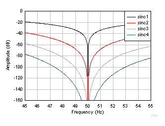
 Figure 72 and Figure 73 plot the detailed frequency response of the 50-SPS and 60-SPS data rates and show various orders of the sinc filter. The high-order sinc filter increases the frequency width of the null, which improves line cycle rejection. Improved 50-Hz or 60-Hz rejection occurs using the sinc3 or sinc4 order filter.
 Figure 72. Sinc Frequency Response, Detailed (50 SPS)
  Figure 73. Sinc Frequency Response, Detailed (60 SPS)
 The sinc filter has an overall low-pass response that rolls off high-frequency components of the signal. The filter bandwidth depends on the output data rate and the order of the output data rate. The overall system bandwidth is the combined responses of the digital filter, the PGA antialias filter, and external signal filters. Table 5 lists the –3-dB bandwidth of the sinc filter.
Table 5. Sinc Filter Bandwidth
| -3-dB BANDWIDTH (Hz) | |||||
|---|---|---|---|---|---|
| DATA RATE (SPS) | SINC1 | SINC2 | SINC3 | SINC4 | SINC5 |
| 2.5 | 1.10 | 0.80 | 0.65 | 0.58 | — |
| 5 | 2.23 | 1.60 | 1.33 | 1.15 | — |
| 10 | 4.43 | 3.20 | 2.62 | 2.28 | — |
| 16.6 | 7.38 | 5.33 | 4.37 | 3.80 | — |
| 20 | 8.85 | 6.38 | 5.25 | 4.63 | — |
| 50 | 22.1 | 16.0 | 13.1 | 11.4 | — |
| 60 | 26.6 | 19.1 | 15.7 | 13.7 | — |
| 100 | 44.3 | 31.9 | 26.2 | 22.8 | — |
| 400 | 177 | 128 | 105 | 91.0 | — |
| 1200 | 525 | 381 | 314 | 273 | — |
| 2400 | 1015 | 751 | 623 | 544 | — |
| 4800 | 1798 | 1421 | 1214 | 1077 | — |
| 7200 | 2310 | 1972 | 1750 | 1590 | — |
| 14400 | — | — | — | — | 2940 |
| 19200 | — | — | — | — | 3920 |
| 25600 | — | — | — | — | 5227 |
| 40000 | — | — | — | — | 8167 |