SBAS937B September 2018 – December 2018 ADS1278-SP
PRODUCTION DATA.
- 1 Features
- 2 Applications
- 3 Description
- 4 Revision History
- 5 Description (continued)
- 6 Pin Configuration and Functions
- 7 Specifications
-
8 Detailed Description
- 8.1 Overview
- 8.2 Functional Block Diagram
- 8.3
Feature Description
- 8.3.1 Sampling Aperture Matching
- 8.3.2 Frequency Response
- 8.3.3 Phase Response
- 8.3.4 Settling Time
- 8.3.5 Data Format
- 8.3.6 Analog Inputs (AINP, AINN)
- 8.3.7 Voltage Reference Inputs (VREFP, VREFN)
- 8.3.8 Clock Input (CLK)
- 8.3.9 Mode Selection (MODE)
- 8.3.10 Synchronization (SYNC)
- 8.3.11 Power-Down (PWDN)
- 8.3.12 Format[2:0]
- 8.3.13 Serial Interface Protocols
- 8.3.14 SPI Serial Interface
- 8.3.15 Frame-Sync Serial Interface
- 8.3.16 DOUT Modes
- 8.3.17 Daisy-Chaining
- 8.3.18 Modulator Output
- 8.3.19 Pin Test Using Test[1:0] Inputs
- 8.3.20 VCOM Output
- 8.4 Device Functional Modes
- 9 Application and Implementation
- 10Power Supply Recommendations
- 11Layout
- 12Device and Documentation Support
- 13Mechanical, Packaging, and Orderable Information
Package Options
Mechanical Data (Package|Pins)
- HFQ|84
Thermal pad, mechanical data (Package|Pins)
Orderable Information
8.3.16.4 Discrete Data Output Mode
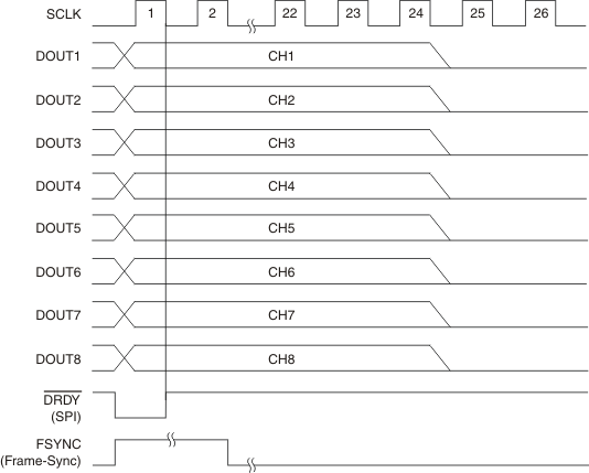
In Discrete data output mode, the channel data are shifted out in parallel using individual channel data output pins DOUT[8:1]. After the 24th SCLK, the channel data are forced to zero. The data are also forced to zero for powered down channels. Figure 76 shows the discrete data output format.
 Figure 74. TDM Mode, Fixed-Position Data (Channels 1 And 3 Shown Powered Down)
  Figure 75. TDM Mode, Dynamic Position Data (Channels 1 And 3 Shown Powered Down)
  Figure 76. Discrete Data Output Mode