SBAS937B September 2018 – December 2018 ADS1278-SP
PRODUCTION DATA.
- 1 Features
- 2 Applications
- 3 Description
- 4 Revision History
- 5 Description (continued)
- 6 Pin Configuration and Functions
- 7 Specifications
-
8 Detailed Description
- 8.1 Overview
- 8.2 Functional Block Diagram
- 8.3
Feature Description
- 8.3.1 Sampling Aperture Matching
- 8.3.2 Frequency Response
- 8.3.3 Phase Response
- 8.3.4 Settling Time
- 8.3.5 Data Format
- 8.3.6 Analog Inputs (AINP, AINN)
- 8.3.7 Voltage Reference Inputs (VREFP, VREFN)
- 8.3.8 Clock Input (CLK)
- 8.3.9 Mode Selection (MODE)
- 8.3.10 Synchronization (SYNC)
- 8.3.11 Power-Down (PWDN)
- 8.3.12 Format[2:0]
- 8.3.13 Serial Interface Protocols
- 8.3.14 SPI Serial Interface
- 8.3.15 Frame-Sync Serial Interface
- 8.3.16 DOUT Modes
- 8.3.17 Daisy-Chaining
- 8.3.18 Modulator Output
- 8.3.19 Pin Test Using Test[1:0] Inputs
- 8.3.20 VCOM Output
- 8.4 Device Functional Modes
- 9 Application and Implementation
- 10Power Supply Recommendations
- 11Layout
- 12Device and Documentation Support
- 13Mechanical, Packaging, and Orderable Information
Package Options
Mechanical Data (Package|Pins)
- HFQ|84
Thermal pad, mechanical data (Package|Pins)
Orderable Information
8.3.10 Synchronization (SYNC)
The ADS1278-SP can be synchronized by pulsing the SYNC pin low and then returning the pin high. When the pin goes low, the conversion process stops, and the internal counters used by the digital filter are reset. When the SYNC pin returns high, the conversion process restarts. Synchronization allows the conversion to be aligned with an external event, such as the changing of an external multiplexer on the analog inputs, or by a reference timing pulse.
Because the ADS1278-SP converters operate in parallel from the same master clock and use the same SYNC input control, they are always in synchronization with each other. The aperture match among internal channels is typically less than 500 ps. However, the synchronization of multiple devices is somewhat different. At device power-on, variations in internal reset thresholds from device to device may result in uncertainty in conversion timing.
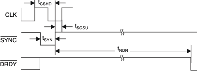
The SYNC pin can be used to synchronize multiple devices to within the same CLK cycle. Figure 69 illustrates the timing requirement of SYNC and CLK in SPI format.
See Figure 70 for the Frame-Sync format timing requirement.
After synchronization, indication of valid data depends on whether SPI or Frame-Sync format was used.
In the SPI format, DRDY goes high as soon as SYNC is taken low; see Figure 69. After SYNC is returned high, DRDY stays high while the digital filter is settling. Once valid data are ready for retrieval, DRDY goes low.
In the Frame-Sync format, DOUT goes low as soon as SYNC is taken low; see Figure 70. After SYNC is returned high, DOUT stays low while the digital filter is settling. Once valid data are ready for retrieval, DOUT begins to output valid data. For proper synchronization, FSYNC, SCLK, and CLK must be established before taking SYNC high, and must then remain running. If the clock inputs (CLK, FSYNC or SCLK) are subsequently interrupted or reset, re-assert the SYNC pin.
For consistent performance, re-assert SYNC after device power-on when data first appear.
 Figure 69. Synchronization Timing (SPI Protocol)
 Table 8. SPI Protocol
| SYMBOL | DESCRIPTION | MIN | TYP | MAX | UNITS |
|---|---|---|---|---|---|
| tCSHD | CLK to SYNC hold time | 10 | ns | ||
| tSCSU | SYNC to CLK setup time | 5 | ns | ||
| tSYN | Synchronize pulse width | 1 | CLK periods | ||
| tNDR | Time for new data to be ready | 129 | Conversions (1/fDATA) |
 Figure 70. Synchronization Timing (Frame-Sync Protocol)
 Table 9. Frame-Sync Protocol
| SYMBOL | DESCRIPTION | MIN | TYP | MAX | UNITS |
|---|---|---|---|---|---|
| tCSHD | CLK to SYNC hold time | 10 | ns | ||
| tSCSU | SYNC to CLK setup time | 5 | ns | ||
| tSYN | Synchronize pulse width | 1 | CLK periods | ||
| tNDR | Time for new data to be ready | 127 | 128 | Conversions (1/fDATA) |