SBAS946C April   2021  – September 2022 ADS127L11

PRODUCTION DATA  

  1. Features
  2. Applications
  3. Description
  4. Revision History
  5. Pin Configuration and Functions
  6. Specifications
    1. 6.1  Absolute Maximum Ratings
    2. 6.2  ESD Ratings
    3. 6.3  Recommended Operating Conditions
    4. 6.4  Thermal Information
    5. 6.5  Electrical Characteristics
    6. 6.6  Timing Requirements (1.65 V ≤ IOVDD ≤ 2 V)
    7. 6.7  Switching Characteristics (1.65 V ≤ IOVDD ≤ 2 V)
    8. 6.8  Timing Requirements (2 V < IOVDD ≤ 5.5 V)
    9. 6.9  Switching Characteristics (2 V < IOVDD ≤ 5.5 V)
    10. 6.10 Timing Diagrams
    11. 6.11 Typical Characteristics
  7. Parameter Measurement Information
    1. 7.1  Offset Error Measurement
    2. 7.2  Offset Drift Measurement
    3. 7.3  Gain Error Measurement
    4. 7.4  Gain Drift Measurement
    5. 7.5  NMRR Measurement
    6. 7.6  CMRR Measurement
    7. 7.7  PSRR Measurement
    8. 7.8  SNR Measurement
    9. 7.9  INL Error Measurement
    10. 7.10 THD Measurement
    11. 7.11 SFDR Measurement
    12. 7.12 Noise Performance
  8. Detailed Description
    1. 8.1 Overview
    2. 8.2 Functional Block Diagram
    3. 8.3 Feature Description
      1. 8.3.1 Analog Input (AINP, AINN)
        1. 8.3.1.1 Input Range
      2. 8.3.2 Reference Voltage (REFP, REFN)
        1. 8.3.2.1 Reference Voltage Range
      3. 8.3.3 Clock Operation
        1. 8.3.3.1 Internal Oscillator
        2. 8.3.3.2 External Clock
      4. 8.3.4 Modulator
      5. 8.3.5 Digital Filter
        1. 8.3.5.1 Wideband Filter
        2. 8.3.5.2 Low-Latency Filter (Sinc)
          1. 8.3.5.2.1 Sinc4 Filter
          2. 8.3.5.2.2 Sinc4 + Sinc1 Filter
          3. 8.3.5.2.3 Sinc3 Filter
          4. 8.3.5.2.4 Sinc3 + Sinc1 Filter
      6. 8.3.6 Power Supplies
        1. 8.3.6.1 AVDD1 and AVSS
        2. 8.3.6.2 AVDD2
        3. 8.3.6.3 IOVDD
        4. 8.3.6.4 Power-On Reset (POR)
        5. 8.3.6.5 CAPA and CAPD
      7. 8.3.7 VCM Output Voltage
    4. 8.4 Device Functional Modes
      1. 8.4.1 Power-Scalable Speed Modes
      2. 8.4.2 Idle Mode
      3. 8.4.3 Standby Mode
      4. 8.4.4 Power-Down Mode
      5. 8.4.5 Reset
        1. 8.4.5.1 RESET Pin
        2. 8.4.5.2 Reset by SPI Register Write
        3. 8.4.5.3 Reset by SPI Input Pattern
      6. 8.4.6 Synchronization
        1. 8.4.6.1 Synchronized Control Mode
        2. 8.4.6.2 Start/Stop Control Mode
        3. 8.4.6.3 One-Shot Control Mode
      7. 8.4.7 Conversion-Start Delay Time
      8. 8.4.8 Calibration
        1. 8.4.8.1 OFFSET2, OFFSET1, OFFSET0 Calibration Registers (Addresses 9h, Ah, Bh)
        2. 8.4.8.2 GAIN2, GAIN1, GAIN0 Calibration Registers (Addresses 0Ch, 0Dh, 0Eh)
        3. 8.4.8.3 Calibration Procedure
    5. 8.5 Programming
      1. 8.5.1 Serial Interface (SPI)
        1. 8.5.1.1 Chip Select (CS)
        2. 8.5.1.2 Serial Clock (SCLK)
        3. 8.5.1.3 Serial Data Input (SDI)
        4. 8.5.1.4 Serial Data Output/Data Ready (SDO/DRDY)
      2. 8.5.2 SPI Frame
      3. 8.5.3 SPI CRC
      4. 8.5.4 Register Map CRC
      5. 8.5.5 Full-Duplex Operation
      6. 8.5.6 Device Commands
        1. 8.5.6.1 No-Operation
        2. 8.5.6.2 Read Register Command
        3. 8.5.6.3 Write Register Command
      7. 8.5.7 Read Conversion Data
        1. 8.5.7.1 Conversion Data
        2. 8.5.7.2 Data Ready
          1. 8.5.7.2.1 DRDY
          2. 8.5.7.2.2 SDO/DRDY
          3. 8.5.7.2.3 DRDY Bit
          4. 8.5.7.2.4 Clock Counting
        3. 8.5.7.3 STATUS Header
      8. 8.5.8 Daisy-Chain Operation
      9. 8.5.9 3-Wire SPI Mode
        1. 8.5.9.1 3-Wire SPI Mode Frame Reset
    6. 8.6 Registers
      1. 8.6.1  DEV_ID Register (Address = 0h) [reset = 00h]
      2. 8.6.2  REV_ID Register (Address = 1h) [reset = xxh]
      3. 8.6.3  STATUS Register (Address = 2h) [reset = x1100xxxb]
      4. 8.6.4  CONTROL Register (Address = 3h) [reset = 00h]
      5. 8.6.5  MUX Register (Address = 4h) [reset = 00h]
      6. 8.6.6  CONFIG1 Register (Address = 5h) [reset = 00h]
      7. 8.6.7  CONFIG2 Register (Address = 6h) [reset = 00h]
      8. 8.6.8  CONFIG3 Register (Address = 7h) [reset = 00h]
      9. 8.6.9  CONFIG4 Register (Address = 8h) [reset = 00h]
      10. 8.6.10 OFFSET2, OFFSET1, OFFSET0 Registers (Addresses = 9h, Ah, Bh) [reset = 00h, 00h, 00h]
      11. 8.6.11 GAIN2, GAIN1, GAIN0 Registers (Addresses = Ch, Dh, Eh) [reset = 40h, 00h, 00h]
      12. 8.6.12 CRC Register (Address = Fh) [reset = 00h]
  9. Application and Implementation
    1. 9.1 Application Information
      1. 9.1.1 SPI Operation
      2. 9.1.2 Input Driver
      3. 9.1.3 Antialias Filter
      4. 9.1.4 Reference Voltage
      5. 9.1.5 Simultaneous-Sampling Systems
    2. 9.2 Typical Application
      1. 9.2.1 Design Requirements
      2. 9.2.2 Detailed Design Procedure
      3. 9.2.3 Application Curves
    3. 9.3 Power Supply Recommendations
    4. 9.4 Layout
      1. 9.4.1 Layout Guidelines
      2. 9.4.2 Layout Example
  10. 10Device and Documentation Support
    1. 10.1 Documentation Support
      1. 10.1.1 Related Documentation
    2. 10.2 Receiving Notification of Documentation Updates
    3. 10.3 Support Resources
    4. 10.4 Trademarks
    5. 10.5 Electrostatic Discharge Caution
    6. 10.6 Glossary
  11. 11Mechanical, Packaging, and Orderable Information

Package Options

Mechanical Data (Package|Pins)
Thermal pad, mechanical data (Package|Pins)
Orderable Information
Sinc3 Filter

The sinc3 filter mode is a single-stage filter. Relatively high values of OSR provide line-cycle rejection with data rates = 480 SPS, 400 SPS, 60 SPS, and 50 SPS. Because of the large width of the frequency response notch, excellent line-frequency NMRR and CMRR can be achieved with this filter. Table 8-7 summarizes the characteristics of the sinc3 filter.

Table 8-7 Sinc3 Filter Characteristics
OSR DATA RATE (SPS) –3-dB FREQUENCY (Hz) LATENCY (ms) REJECTION OF FIRST NULL (dB)
2% CLOCK TOLERANCE 6% CLOCK TOLERANCE
HIGH-SPEED MODE (fCLK = 25.6 MHz)
26667 480 126 6.25 100 71
32000 400 105 7.50 100 71
LOW-SPEED MODE (fCLK = 3.2 MHz)
26667 60 15.7 50.01 100 71
32000 50 13.1 60.01 100 71

Figure 8-17 shows the frequency response of the sinc3 filter (OSR = 32000). Figure 8-18 shows the detailed response in the region of 0.9 to 1.1 · fIN / fDATA.
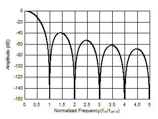
GUID-20201006-CA0I-2CSD-6XTF-4HPBXJRNNG2K-low.gifFigure 8-17 Sinc3 Frequency Response
(OSR = 32000)
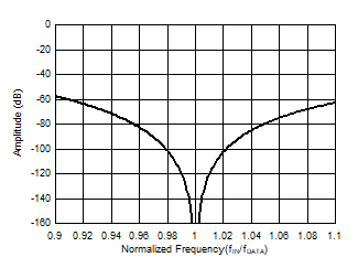
GUID-20201006-CA0I-VJD0-PKS7-FQJH9W12PBQH-low.gifFigure 8-18 Detail Sinc3 Frequency Response (OSR = 32000)