SBASAM0B March   2024  – November 2024 ADS127L18

PRODMIX  

  1.   1
  2. Features
  3. Applications
  4. Description
  5. Pin Configuration and Functions
  6. Specifications
    1. 5.1 Absolute Maximum Ratings
    2. 5.2 ESD Ratings
    3. 5.3 Recommended Operating Conditions
    4. 5.4 Thermal Information
    5. 5.5 Electrical Characteristics
    6. 5.6 Timing Requirements
    7. 5.7 Switching Characteristics
    8. 5.8 Timing Diagrams
    9. 5.9 Typical Characteristics
  7. Parameter Measurement Information
    1. 6.1  Offset Error Measurement
    2. 6.2  Offset Drift Measurement
    3. 6.3  Gain Error Measurement
    4. 6.4  Gain Drift Measurement
    5. 6.5  NMRR Measurement
    6. 6.6  CMRR Measurement
    7. 6.7  PSRR Measurement
    8. 6.8  SNR Measurement
    9. 6.9  INL Error Measurement
    10. 6.10 THD Measurement
    11. 6.11 IMD Measurement
    12. 6.12 SFDR Measurement
    13. 6.13 Noise Performance
  8. Detailed Description
    1. 7.1 Overview
    2. 7.2 Functional Block Diagram
    3. 7.3 Feature Description
      1. 7.3.1 Analog Inputs (AINP, AINN)
        1. 7.3.1.1 Input Range
      2. 7.3.2 Reference Voltage (REFP, REFN)
        1. 7.3.2.1 Reference Voltage Range
      3. 7.3.3 Clock Operation
        1. 7.3.3.1 Clock Dividers
        2. 7.3.3.2 Internal Oscillator
        3. 7.3.3.3 External Clock
      4. 7.3.4 Power-On Reset (POR)
      5. 7.3.5 VCM Output Voltage
      6. 7.3.6 GPIO
      7. 7.3.7 Modulator
      8. 7.3.8 Digital Filter
        1. 7.3.8.1 Wideband Filter
        2. 7.3.8.2 Low-Latency Filter (Sinc)
          1. 7.3.8.2.1 Sinc4 Filter
          2. 7.3.8.2.2 Sinc4 + Sinc1 Cascade Filter
          3. 7.3.8.2.3 Sinc3 Filter
          4. 7.3.8.2.4 Sinc3 + Sinc1 Filter
    4. 7.4 Device Functional Modes
      1. 7.4.1  Reset
        1. 7.4.1.1 RESET Pin
        2. 7.4.1.2 Reset by SPI Register
        3. 7.4.1.3 Reset by SPI Input Pattern
      2. 7.4.2  Idle and Standby Modes
      3. 7.4.3  Power-Down
      4. 7.4.4  Speed Modes
      5. 7.4.5  Synchronization
        1. 7.4.5.1 Synchronized Control Mode
        2. 7.4.5.2 Start/Stop Control Mode
      6. 7.4.6  Conversion-Start Delay Time
      7. 7.4.7  Calibration
        1. 7.4.7.1 Offset Calibration Registers
        2. 7.4.7.2 Gain Calibration Registers
        3. 7.4.7.3 Calibration Procedure
      8. 7.4.8  Data Averaging
      9. 7.4.9  Diagnostics
        1. 7.4.9.1 ERROR Pin and ERR_FLAG Bit
        2. 7.4.9.2 SPI CRC
        3. 7.4.9.3 Register Map CRC
        4. 7.4.9.4 ADC Error
        5. 7.4.9.5 SPI Address Range
        6. 7.4.9.6 SCLK Counter
        7. 7.4.9.7 Clock Counter
        8. 7.4.9.8 Frame-Sync CRC
        9. 7.4.9.9 Self Test
      10. 7.4.10 Frame-Sync Data Port
        1. 7.4.10.1  Data Packet
        2. 7.4.10.2  Data Format
        3. 7.4.10.3  STATUS_DP Header Byte
        4. 7.4.10.4  FSYNC Pin
        5. 7.4.10.5  DCLK Pin
        6. 7.4.10.6  DOUTx Pins
        7. 7.4.10.7  DINx Pins
        8. 7.4.10.8  Time Division Multiplexing
        9. 7.4.10.9  Daisy Chain
        10. 7.4.10.10 DOUTx Timing
    5. 7.5 Programming
      1. 7.5.1 Hardware Programming
      2. 7.5.2 SPI Programming
        1. 7.5.2.1 Chip Select (CS)
        2. 7.5.2.2 Serial Clock (SCLK)
        3. 7.5.2.3 Serial Data Input (SDI)
        4. 7.5.2.4 Serial Data Output (SDO)
      3. 7.5.3 SPI Frame
      4. 7.5.4 Commands
        1. 7.5.4.1 Write Register Command
        2. 7.5.4.2 Read Register Command
      5. 7.5.5 SPI Daisy-Chain
  9. Register Map
  10. Application and Implementation
    1. 9.1 Application Information
      1. 9.1.1 Input Driver
      2. 9.1.2 Antialias Filter
      3. 9.1.3 Reference Voltage
    2. 9.2 Typical Application
      1. 9.2.1 Design Requirements
      2. 9.2.2 Detailed Design Procedure
      3. 9.2.3 Application Curves
    3. 9.3 Power Supply Recommendations
      1. 9.3.1 AVDD1 and AVSS
      2. 9.3.2 AVDD2
      3. 9.3.3 IOVDD
      4. 9.3.4 CAPA and CAPD
    4. 9.4 Layout
      1. 9.4.1 Layout Guidelines
      2. 9.4.2 Layout Example
  11. 10Device and Documentation Support
    1. 10.1 Documentation Support
      1. 10.1.1 Related Documentation
    2. 10.2 Receiving Notification of Documentation Updates
    3. 10.3 Support Resources
    4. 10.4 Trademarks
    5. 10.5 Electrostatic Discharge Caution
    6. 10.6 Glossary
  12. 11Revision History
  13. 12Mechanical, Packaging, and Orderable Information

Package Options

Mechanical Data (Package|Pins)
Thermal pad, mechanical data (Package|Pins)
Orderable Information
Sinc3 Filter

The sinc3 filter mode is a single-stage filter. The sinc3 filter provides several data rate options including 400SPS, 60SPS, and 50SPS for line-cycle noise rejection. 10SPS is achieved by slowing the ADC clock to 10/50 x 3.2MHz = 0.64MHz in low-speed mode. Because of the large width of the frequency response notch, excellent line-frequency NMRR and CMRR is achieved. Table 7-6 summarizes the characteristics of the sinc3 filter.

Table 7-6 Sinc3 Filter Characteristics
MODE fCLK
(MHz)
OSR DATA RATE (SPS) –3dB FREQUENCY (Hz) LATENCY
(ms)
NMRR AT FIRST NULL (dB)
2% CLOCK TOLERANCE 6% CLOCK TOLERANCE
Max speed 32.768 26667 614.4 161.3 4.88 100 71
High speed 25.6 480 126 6.25
Mid speed 12.8 240 63.0 12.5
Low speed 3.2 60 15.7 50.0
Max speed 32.768 32000 512 134 5.86 100 71
High speed 25.6 400 105 7.50
Mid speed 12.8 200 252 15
Low speed 3.2 50 13.1 60.0

Figure 7-21 shows the frequency response of the sinc3 filter (OSR = 32000). Figure 7-22 shows the detailed response in the region of 0.9 to 1.1 · fIN / fDATA.
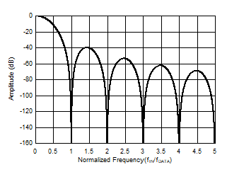
ADS127L14 ADS127L18 Sinc3 Frequency Response
                            (OSR = 32000)Figure 7-21 Sinc3 Frequency Response
(OSR = 32000)
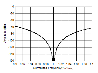
ADS127L14 ADS127L18 Detail Sinc3 Frequency Response (OSR = 32000)Figure 7-22 Detail Sinc3 Frequency Response (OSR = 32000)