SBASAM0B March 2024 – November 2024 ADS127L18
PRODMIX
- 1
- 1 Features
- 2 Applications
- 3 Description
- 4 Pin Configuration and Functions
- 5 Specifications
-
6 Parameter Measurement Information
- 6.1 Offset Error Measurement
- 6.2 Offset Drift Measurement
- 6.3 Gain Error Measurement
- 6.4 Gain Drift Measurement
- 6.5 NMRR Measurement
- 6.6 CMRR Measurement
- 6.7 PSRR Measurement
- 6.8 SNR Measurement
- 6.9 INL Error Measurement
- 6.10 THD Measurement
- 6.11 IMD Measurement
- 6.12 SFDR Measurement
- 6.13 Noise Performance
-
7 Detailed Description
- 7.1 Overview
- 7.2 Functional Block Diagram
- 7.3 Feature Description
- 7.4 Device Functional Modes
- 7.5 Programming
- 8 Register Map
- 9 Application and Implementation
- 10Device and Documentation Support
- 11Revision History
- 12Mechanical, Packaging, and Orderable Information
Package Options
Mechanical Data (Package|Pins)
- RSH|56
Thermal pad, mechanical data (Package|Pins)
Orderable Information
7.3.8.2.1 Sinc4 Filter
The sinc4 filter performs averaging and decimation of the modulator data to produce data rates up to 1365.3kSPS in max-speed mode, 1066.6kSPS in high-speed mode, 533.3kSPS in mid-speed mode and 133.333kSPS in low-speed mode. Increasing the OSR value decreases the ADC data rate that reduces signal bandwidth and total noise resulting from increased data averaging and decimation.
Table 7-20 lists the sinc4 filter characteristics.
| MODE | fCLK (MHz) |
OSR | DATA RATE (kSPS) |
–3-dB FREQUENCY (kHz) |
LATENCY TIME (μs)(1) |
|---|---|---|---|---|---|
| Max speed | 32.768 | 12 | 1365.3 | 310.2 | 3.9 |
| High speed | 25.6 | 1066.6 | 242.3 | 5.1 | |
| Mid speed | 12.8 | 533.3 |
121.2 | 10.1 | |
| Low speed | 3.2 | 133.33 | 30.3 | 40.5 | |
| Max speed | 32.768 | 16 | 1024 | 232.7 | 4.9 |
| High speed | 25.6 | 800 | 181.8 | 6.3 | |
| Mid speed | 12.8 | 400 | 90.9 | 12.6 | |
| Low speed | 3.2 | 100 | 22.7 | 50.5 | |
| Max speed | 32.768 | 24 | 682.67 | 155.1 | 6.9 |
| High speed | 25.6 | 533.3 | 121.2 | 8.9 | |
| Mid speed | 12.8 | 266.67 | 60.6 | 17.1 | |
| Low speed | 3.2 | 66.67 | 15.1 | 70.8 | |
| Max speed | 32.768 | 32 | 512 | 116.3 | 8.9 |
| High speed | 25.6 | 400 | 90.9 | 11.4 | |
| Mid speed | 12.8 | 200 | 45.4 | 22.8 | |
| Low speed | 3.2 | 50 | 11.4 | 91.4 | |
| Max speed | 32.768 | 64 | 256 | 58.2 | 16.6 |
| High speed | 25.6 | 200 | 45.4 | 21.3 | |
| Mid speed | 12.8 | 100 | 22.7 | 42.6 | |
| Low speed | 3.2 | 25 | 5.68 | 171 | |
| Max speed | 32.768 | 128 | 128 | 29.1 | 32.3 |
| High speed | 25.6 | 100 | 22.7 | 41.3 | |
| Mid speed | 12.8 | 50 | 11.4 | 82.6 | |
| Low speed | 3.2 | 12.5 | 2.84 | 331 | |
| Max speed | 32.768 | 256 | 64 | 14.5 | 63.6 |
| High speed | 25.6 | 50 | 11.4 | 81.4 | |
| Mid speed | 12.8 | 25 | 5.68 | 163 | |
| Low speed | 3.2 | 6.25 | 1.42 | 651 | |
| Max speed | 32.768 | 512 | 32 | 7.27 | 126 |
| High speed | 25.6 | 25 | 5.68 | 162 | |
| Mid speed | 12.8 | 12.5 | 2.84 | 324 | |
| Low speed | 3.2 | 3.125 | 0.710 | 1294 | |
| Max speed | 32.768 | 1024 | 16 | 3.64 | 251 |
| High speed | 25.6 | 12.5 | 2.84 | 321 | |
| Mid speed | 12.8 | 6.25 | 1.42 | 643 | |
| Low speed | 3.2 | 1.5625 | 0.355 | 2570 | |
| Max speed | 32.768 | 2048 | 8 | 1.82 | 501 |
| High speed | 25.6 | 6.25 | 1.42 | 641 | |
| Mid speed | 12.8 | 3.125 | 0.710 | 1282 | |
| Low speed | 3.2 | 0.7813 | 0.178 | 5130 | |
| Max speed | 32.768 | 4096 | 4 | 0.909 | 1001 |
| High speed | 25.6 | 3.125 | 0.710 | 1281 | |
| Mid speed | 12.8 | 1.563 | 0.355 | 2562 | |
| Low speed | 3.2 | 0.391 | 0.089 | 10250 |
Because the amount of data averaging is reduced for OSR values equal to 12, 16, and 24, full 24-bit output data resolution is not available. Table 7-4 summarizes the output data resolution for low OSR values.
| OSR | RESOLUTION (BITS) |
|---|---|
| 12 | 19 |
| 16 | 20 |
| 24 | 23 |
| ≥32 | 24 |
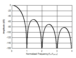
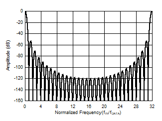
Figure 7-18 and Figure 7-19 show the sinc4 frequency response for OSR = 32. The frequency response consists of a series of response nulls occurring at multiples of fDATA with a series of decaying peaks in between. At the null frequencies, the filter has zero gain. A folded image of the filter response appears when fIN/fDATA > OSR/2, as illustrated in the frequency plot of Figure 7-19 for OSR = 32. 0dB attenuation occurs at input frequencies near n × fMOD (n = 1, 2, 3, and so on). If signals are present at these frequencies, the signal is aliased to the pass band.
 Figure 7-18 Sinc4 Frequency
Response
Figure 7-18 Sinc4 Frequency
Response(OSR = 32)
 Figure 7-19 Sinc4 Frequency Response
to fMOD (OSR = 32)