SBASB74 October 2024 ADS127L21B
PRODUCTION DATA
- 1
- 1 Features
- 2 Applications
- 3 Description
- 4 Pin Configuration and Functions
-
5 Specifications
- 5.1 Absolute Maximum Ratings
- 5.2 ESD Ratings
- 5.3 Recommended Operating Conditions
- 5.4 Thermal Information
- 5.5 Electrical Characteristics
- 5.6 Timing Requirements (1.65V ≤ IOVDD ≤ 2V)
- 5.7 Switching Characteristics (1.65V ≤ IOVDD ≤ 2V)
- 5.8 Timing Requirements (2V < IOVDD ≤ 5.5V)
- 5.9 Switching Characteristics (2V < IOVDD ≤ 5.5V)
- 5.10 Timing Diagrams
- 5.11 Typical Characteristics
-
6 Parameter Measurement Information
- 6.1 Offset Error Measurement
- 6.2 Offset Drift Measurement
- 6.3 Gain Error Measurement
- 6.4 Gain Drift Measurement
- 6.5 NMRR Measurement
- 6.6 CMRR Measurement
- 6.7 PSRR Measurement
- 6.8 SNR Measurement
- 6.9 INL Error Measurement
- 6.10 THD Measurement
- 6.11 IMD Measurement
- 6.12 SFDR Measurement
- 6.13 Noise Performance
-
7 Detailed Description
- 7.1 Overview
- 7.2 Functional Block Diagram
- 7.3 Feature Description
- 7.4 Device Functional Modes
- 7.5
Programming
- 7.5.1
Serial Interface (SPI)
- 7.5.1.1 Chip Select (CS)
- 7.5.1.2 Serial Clock (SCLK)
- 7.5.1.3 Serial Data Input (SDI)
- 7.5.1.4 Serial Data Output/Data Ready (SDO/DRDY)
- 7.5.1.5 SPI Frame
- 7.5.1.6 Full-Duplex Operation
- 7.5.1.7 Device Commands
- 7.5.1.8 Read Conversion Data
- 7.5.1.9 Daisy-Chain Operation
- 7.5.1.10 3-Wire SPI Mode
- 7.5.1.11 SPI CRC
- 7.5.2 Register Memory CRC
- 7.5.1
Serial Interface (SPI)
- 8 Register Map
- 9 Application and Implementation
- 10Device and Documentation Support
- 11Revision History
- 12Mechanical, Packaging, and Orderable Information
Package Options
Mechanical Data (Package|Pins)
- RUK|20
Thermal pad, mechanical data (Package|Pins)
- RUK|20
Orderable Information
7.3.5.1.6 FIR3 Default Coefficients
FIR3 coefficients are available without the need to supply custom coefficients. The default coefficients are selected by the FLTR_SEL[2:0] bits = 000b of the FILTER1 register. The default coefficients feature linear phase response, low pass-band ripple, narrow transition band, and high stop-band attenuation.
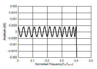
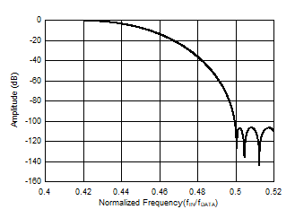
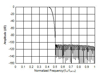
Figure 7-14 through Figure 7-18 illustrate the default wideband filter frequency response. Figure 7-14 shows the pass-band ripple. Figure 7-15 shows the frequency response at the transition band.
 Figure 7-14 Wideband Filter Pass-Band
Ripple
 Figure 7-15 Wideband Filter Transition
Band
Figure 7-15 Wideband Filter Transition
BandFigure 7-16 illustrates the filter response up to fDATA for OSR ≥ 64. The stop band begins at fDATA / 2 to reduce signal aliasing. Figure 7-17 illustrates the filter to fMOD. In the stop-band region, signal frequencies intermodulate with multiples of the chop frequency at fMOD / 32. Thus, creating a series of response peaks that exceed the attenuation provided by the digital filter. The width of the response peaks is twice the filter bandwidth. Stop-band attenuation is improved when the ADC input is filtered by an analog antialias filter. See the THS4551 Antialias Filter Design section for details of a fourth-order antialias filter at the ADC input.

| OSR ≥ 64 |

| OSR = 32 |
Figure 7-18 shows the filter response at fMOD. As shown, the filter response repeats for input signals at fMOD. If not removed by an antialias filter, signal frequencies at fMOD appear as aliased frequencies in the pass band.
 Figure 7-18 Wideband Filter
Frequency Response at fMOD
Figure 7-18 Wideband Filter
Frequency Response at fMODAliasing also occurs with input frequencies occurring at multiples of fMOD. These frequency bands are defined by:
where:
- N = 1, 2, 3, and so on
- fMOD = Modulator sampling frequency
- fBW = Filter bandwidth
The group delay of the filter is the propagation time for an input signal to appear at the output of the filter. Because the filter is a linear-phase design, the envelope of a complex input signal is undistorted by the filter. The group delay (expressed in units of time) is constant versus frequency, equal to 34 / fDATA. After a step input is applied, fully settled data occur 68 data periods later. Figure 7-19 illustrates the filter group delay (34 / fDATA) and the settling time to a step input (68 / fDATA).
 Figure 7-19 Wideband Filter Step Response
The digital filter is restarted when the ADC is synchronized. The ADC suppresses the first 68 conversion periods until the filter is fully settled. There is no need to discard data after synchronization. The time of data suppression is the conversion latency time as listed in the latency time column of Table 7-12. Sixteen fCLK cycles of overhead time are incurred for all data rates. If a step input is applied randomly to the conversion period without synchronizing, the next 69 conversions are unsettled data. The –0.1dB frequency of the amplitude response is 0.4125 × fDATA and the –3dB frequency is 0.4374 × fDATA for all data rates.
| MODE | fCLK (MHz) | OSR | DATA RATE (kSPS) | –0.1dB FREQUENCY (kHz) | –3dB FREQUENCY (kHz) | LATENCY TIME(1) (µs) |
|---|---|---|---|---|---|---|
| Max speed | 32.768 | 32 | 512 | 211.2 | 223.9 | 135.5 |
| High speed | 25.6 | 400 | 165 | 174.96 | 173.4 | |
| Mid speed | 12.8 | 200 | 82.5 | 87.48 | 346.9 | |
| Low speed | 3.2 | 50 | 20.63 | 21.87 | 1387.8 | |
| Max speed | 32.768 | 64 | 256 | 105.6 | 112.0 | 270.4 |
| High speed | 25.6 | 200 | 82.5 | 87.48 | 346.1 | |
| Mid speed | 12.8 | 100 | 41.25 | 43.74 | 692.2 | |
| Low speed | 3.2 | 25 | 10.31 | 10.94 | 2768.7 | |
| Max speed | 32.768 | 128 | 128 | 52.8 | 55.99 | 540.0 |
| High speed | 25.6 | 100 | 41.25 | 43.74 | 691.2 | |
| Mid speed | 12.8 | 50 | 20.63 | 21.87 | 1382.3 | |
| Low speed | 3.2 | 12.5 | 5.1562 | 5.468 | 5529.2 | |
| Max speed | 32.768 | 256 | 64 | 26.4 | 28.00 | 1079.2 |
| High speed | 25.6 | 50 | 20.625 | 21.87 | 1381.3 | |
| Mid speed | 12.8 | 25 | 10.31 | 10.93 | 2762.6 | |
| Low speed | 3.2 | 6.25 | 2.578 | 2.734 | 11051 | |
| Max speed | 32.768 | 512 | 32 | 13.2 | 14.00 | 2157.6 |
| High speed | 25.6 | 25 | 10.312 | 10.935 | 2761.6 | |
| Mid speed | 12.8 | 12.5 | 5.156 | 5.467 | 5523.3 | |
| Low speed | 3.2 | 3.125 | 1.289 | 1.367 | 22093 | |
| Max speed | 32.768 | 1024 | 16 | 6.6 | 7.998 | 4314.2 |
| High speed | 25.6 | 12.5 | 5.156 | 5.467 | 5522.3 | |
| Mid speed | 12.8 | 6.25 | 2.578 | 2.734 | 11045 | |
| Low speed | 3.2 | 1.5625 | 0.645 | 0.6834 | 44178 | |
| Max speed | 32.768 | 2048 | 8 | 3.3 | 3.499 | 8627.8 |
| High speed | 25.6 | 6.25 | 2.578 | 2.734 | 11044 | |
| Mid speed | 12.8 | 3.125 | 1.289 | 1.367 | 22087 | |
| Low speed | 3.2 | 0.78125 | 0.322 | 0.3417 | 88348 | |
| Max speed | 32.768 | 4096 | 4 | 1.65 | 1.750 | 17254 |
| High speed | 25.6 | 3.125 | 1.289 | 1.367 | 22086 | |
| Mid speed | 12.8 | 1.5625 | 0.645 | 0.6834 | 44172 | |
| Low speed | 3.2 | 0.390625 | 0.161 | 0.1709 | 176690 |