SBASB74 October 2024 ADS127L21B
PRODUCTION DATA
- 1
- 1 Features
- 2 Applications
- 3 Description
- 4 Pin Configuration and Functions
-
5 Specifications
- 5.1 Absolute Maximum Ratings
- 5.2 ESD Ratings
- 5.3 Recommended Operating Conditions
- 5.4 Thermal Information
- 5.5 Electrical Characteristics
- 5.6 Timing Requirements (1.65V ≤ IOVDD ≤ 2V)
- 5.7 Switching Characteristics (1.65V ≤ IOVDD ≤ 2V)
- 5.8 Timing Requirements (2V < IOVDD ≤ 5.5V)
- 5.9 Switching Characteristics (2V < IOVDD ≤ 5.5V)
- 5.10 Timing Diagrams
- 5.11 Typical Characteristics
-
6 Parameter Measurement Information
- 6.1 Offset Error Measurement
- 6.2 Offset Drift Measurement
- 6.3 Gain Error Measurement
- 6.4 Gain Drift Measurement
- 6.5 NMRR Measurement
- 6.6 CMRR Measurement
- 6.7 PSRR Measurement
- 6.8 SNR Measurement
- 6.9 INL Error Measurement
- 6.10 THD Measurement
- 6.11 IMD Measurement
- 6.12 SFDR Measurement
- 6.13 Noise Performance
-
7 Detailed Description
- 7.1 Overview
- 7.2 Functional Block Diagram
- 7.3 Feature Description
- 7.4 Device Functional Modes
- 7.5
Programming
- 7.5.1
Serial Interface (SPI)
- 7.5.1.1 Chip Select (CS)
- 7.5.1.2 Serial Clock (SCLK)
- 7.5.1.3 Serial Data Input (SDI)
- 7.5.1.4 Serial Data Output/Data Ready (SDO/DRDY)
- 7.5.1.5 SPI Frame
- 7.5.1.6 Full-Duplex Operation
- 7.5.1.7 Device Commands
- 7.5.1.8 Read Conversion Data
- 7.5.1.9 Daisy-Chain Operation
- 7.5.1.10 3-Wire SPI Mode
- 7.5.1.11 SPI CRC
- 7.5.2 Register Memory CRC
- 7.5.1
Serial Interface (SPI)
- 8 Register Map
- 9 Application and Implementation
- 10Device and Documentation Support
- 11Revision History
- 12Mechanical, Packaging, and Orderable Information
Package Options
Mechanical Data (Package|Pins)
- RUK|20
Thermal pad, mechanical data (Package|Pins)
- RUK|20
Orderable Information
7.3.1 Analog Input (AINP, AINN)
The analog input of the ADC is differential, with the input defined as a difference voltage: VIN = VAINP – VAINN. For best performance, drive the input with a differential signal with the common-mode voltage centered to mid-supply (AVDD1 + AVSS) / 2.
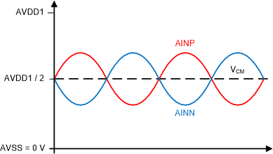
The ADC accepts either unipolar or bipolar input signals by configuring the AVDD1 and AVSS power supplies accordingly. Figure 7-1 shows an example of a differential signal with the supplies configured to unipolar operation. Symmetric input voltage headroom is available when the common-mode voltage is at mid-supply (AVDD1 / 2). Use AVDD1 = 5V and AVSS = 0V for unipolar operation (see specifications for reduced AVDD1 operation).
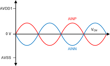
Figure 7-2 shows an example of a differential signal in bipolar operation. The common-mode voltage of the signal (VCM) is normally at 0V. Use AVDD1 = 2.5V and AVSS = –2.5V for bipolar operation.
 Figure 7-1 Unipolar Differential
Input Signal
 Figure 7-2 Bipolar Differential Input
Signal
Figure 7-2 Bipolar Differential Input
SignalIn either bipolar or unipolar power-supply configuration, the ADC accepts single-ended input signals by tying the AINN input to AVSS, ground, or mid-supply. However, because AINN is now fixed, the voltage range of the ADC is limited by the input voltage swing of AINP. That is, ±2.5V for bipolar operation or 0V to 5V for a 5V unipolar operation.
The simplified circuit shown in Figure 7-3 represents the analog input structure.
 Figure 7-3 Analog Input Circuit
Diodes protect the ADC inputs from electrostatic discharge (ESD) events. These events occur during the manufacturing process and during printed circuit board (PCB) assembly when manufactured in an ESD-controlled environment. If the inputs are driven below AVSS – 0.3V, or above AVDD1 + 0.3V, the protection diodes potentially conduct. If these conditions are possible, use external clamp diodes, series resistors, or both to limit the input current to the specified value.
The input multiplexer offers the option of normal or reverse input signal polarities. The multiplexer also provides two internal test modes to help verify ADC performance. The offset test mode verifies noise and offset error by providing a short to the ADC inputs. The resulting noise and offset voltage data are evaluated by the user. CMRR performance is tested using the CMRR test mode by applying a CMRR test signal to the AINP input. The resulting CMRR test data are also evaluated by the user. Table 7-1 shows the switch configurations of the input multiplexer circuit of Figure 7-3.
| MUX[1:0] BITS | CLOSED SWITCHES | DESCRIPTION |
|---|---|---|
| 00b | S1, S4 | Normal polarity input (VIN = VAINP - VAINN) |
| 01b | S2, S3 | Reverse polarity input (VIN = VAINN - VAINP) |
| 10b | S5, S6 | Internal noise and offset error test |
| 11b | S1, S5 | CMRR test using a signal applied to AINP |
The ADC samples the input voltage at the modulator frequency (fMOD) by storing the voltage on the CIN capacitor. The capacitor is discharged on the opposite clock phase of the modulator, at which time the sample process repeats. The instantaneous charge demand of CIN requires the signal to settle within a half cycle at the modulator frequency. This frequency is t = 1 / (2 · fMOD). To satisfy this requirement, the external driver bandwidth is typically required to be much larger than the original signal frequency. The bandwidth of the driver is determined sufficient when the desired THD, SNR, and gain error performance are achieved. In mid- and low-speed modes of operation, the modulator frequency is reduced, therefore more time is available for the driver to settle.
The input charge required by the sampling capacitor is modeled as a peak current and an average current flowing into the ADC inputs. As given in Equation 15 and Equation 16, the average input current is comprised of differential and absolute components.
where:
- fMOD = fCLK / 2
- CIN = 7.4pF (1x input range), 3.6pF (2x input range)
where:
- fMOD = fCLK / 2
- CCM = 0.35pF (1x input range), 0.17pF (2x input range)
For fMOD = 12.8MHz (high-speed mode), CIN = 7.4pF, and CCM = 0.35pF, the average current resulting from the differential voltage is 95μA/V. The average current resulting from the absolute voltage is 4.5μA/V. For example, if AINP = 4.5V and AINN = 0.5V, then VIN = 4V. The total AINP average current = (4V · 95μA/V) + (4.5V · 4.5μA/V) = 400μA. The total AINN average current is (–4V · 95μA/V) + (0.5V · 4.5μA/V) = –378μA.
The device incorporates input precharge buffers to significantly reduce the charge demand from the CIN capacitor. When enabled, the buffers are initially in-circuit during the sampling phase. When CIN is nearly fully charged, the buffers are bypassed (S7 and S8 of Figure 7-3 in up positions). The external signal then provides the fine charge to the capacitor. At the completion of the sample phase, the sampling capacitor is discharged by the modulator to complete the conversion cycle. The buffers reduce the input current required to charge CIN, therefore improving the input impedance and relaxing external driver requirements. The input buffers are enabled by the AINP_BUF and AINN_BUF bits of the CONFIG1 register. If AINN is tied to ground or to a low-impedance fixed potential, disable the AINN buffer to reduce power consumption.