SBAS691B March 2016 – October 2018 ADS1282-SP
PRODUCTION DATA.
- 1 Features
- 2 Applications
- 3 Description
- 4 Revision History
- 5 Description (continued)
- 6 Pin Configuration and Functions
-
7 Specifications
- 7.1 Absolute Maximum Ratings
- 7.2 ESD Ratings
- 7.3 Recommended Operating Conditions
- 7.4 Thermal Information
- 7.5 Electrical Characteristics
- 7.6 Timing Requirements
- 7.7 Pulse-Sync Timing Requirements
- 7.8 Reset Timing Requirements
- 7.9 Read Data Timing Requirements
- 7.10 Switching Characteristics
- 7.11 Typical Characteristics
-
8 Detailed Description
- 8.1 Overview
- 8.2 Functional Block Diagram
- 8.3
Feature Description
- 8.3.1 Noise Performance
- 8.3.2 Input-Referred Noise
- 8.3.3 Idle Tones
- 8.3.4 Operating Mode
- 8.3.5 Analog Inputs and Multiplexer
- 8.3.6 PGA (Programmable Gain Amplifier)
- 8.3.7 ADC
- 8.3.8 Modulator
- 8.3.9 Modulator Over-Range
- 8.3.10 Modulator Input Impedance
- 8.3.11 Modulator Over-Range Detection (MFLAG)
- 8.3.12 Voltage Reference Inputs (VREFP, VREFN)
- 8.3.13 Digital Filter
- 8.3.14 Master Clock Input (CLK)
- 8.3.15 Synchronization (SYNC Pin and Sync Command)
- 8.3.16 Pulse-Sync Mode
- 8.3.17 Continuous-Sync Mode
- 8.3.18 Reset (RESET Pin and Reset Command)
- 8.3.19 Power-Down (PWDN Pin and Standby Command)
- 8.3.20 Power-On Sequence
- 8.3.21 Serial Interface
- 8.3.22 Data Format
- 8.3.23 Reading Data
- 8.3.24 One-Shot Operation
- 8.4 Device Functional Modes
- 8.5
Programming
- 8.5.1
Commands
- 8.5.1.1 WAKEUP: Wake-Up from Standby Mode
- 8.5.1.2 STANDBY: Standby Mode
- 8.5.1.3 SYNC: Synchronize the A/D Conversion
- 8.5.1.4 RESET: Reset the Device
- 8.5.1.5 RDATAC: Read Data Continuous
- 8.5.1.6 SDATAC: Stop Read Data Continuous
- 8.5.1.7 RDATA: Read Data By Command
- 8.5.1.8 RREG: Read Register Data
- 8.5.1.9 WREG: Write to Register
- 8.5.1.10 OFSCAL: Offset Calibration
- 8.5.1.11 GANCAL: Gain Calibration
- 8.5.2 Calibration Commands
- 8.5.3 User Calibration
- 8.5.4 Configuration Guide
- 8.5.1
Commands
- 8.6 Register Maps
- 9 Application and Implementation
- 10Power Supply Recommendations
- 11Layout
- 12Device and Documentation Support
- 13Mechanical, Packaging, and Orderable Information
Package Options
Mechanical Data (Package|Pins)
- HKV|28
Thermal pad, mechanical data (Package|Pins)
Orderable Information
9.2.1.2 Detailed Design Procedure
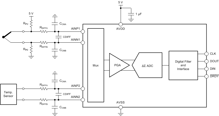
Figure 79 below shows a typical thermocouple application utilizing both analog inputs to the ADS1282-SP; one for hot junction and one for cold junction. The biasing resistors (RPU and RPD) serve two purposes. The first purpose is to set the common-mode voltage of the thermocouple to within the specified voltage range of the device. The second purpose is to offer a weak pullup and pulldown to detect an open thermocouple lead. When one of the thermocouple leads fails open, the positive input is pulled to AVDD and the negative input is pulled to GND. The ADC consequently reads a full-scale value that is outside the normal measurement range of the thermocouple voltage to indicate this failure condition. When choosing the values of the biasing resistors, take care so that the biasing current does not degrade measurement accuracy. The biasing current flows through the thermocouple and can cause self-heating and additional voltage drops across the thermocouple leads. Typical values for the biasing resistors range from 1 MΩ to 50 MΩ.
 Figure 79. ADS1282-SP with Hot and Cold Junction Sensing
 Although the device digital filter attenuates high-frequency components of noise, provide a first-order, passive RC filter at the inputs to further improve performance. The differential RC filter formed by RDIFFA, RDIFFB, and the differential capacitor CDIFF offers a cutoff frequency that is calculated using Equation 15. Care must be taken when choosing the filter resistor values because the input currents flowing into and out of the device cause a voltage drop across the resistors. This voltage drop shows up as an additional offset error at the ADC inputs. Limit the filter resistor values to below 1 kΩ for best performance.
Two common-mode filter capacitors (CCMA and CCMB) are also added to offer attenuation of high-frequency, common-mode noise components. Differential capacitor CDIFF must be at least an order of magnitude (10x) larger than these common-mode capacitors because mismatches in the common mode capacitors can convert common-mode noise into differential noise.
The highest measurement resolution is achieved when the largest potential input signal is slightly lower than the FSR of the ADC. For a type K thermocouple, the maximum thermocouple voltage (VTC) occurs at a thermocouple temperature (TTC) of 1370°C. At this temperature, VTC = 54.819 mV, as defined in the tables published by the National Institute of Standards and Technology (NIST) using a cold-junction temperature (TCJ) of 0°C. A thermocouple produces an output voltage that is proportional to the temperature difference between the thermocouple tip and the cold junction. If the cold junction is at a temperature below 0°C, the thermocouple produces a voltage larger than 54.819 mV. The isothermal block area is often constrained by the operating temperature range of the device. Therefore, the isothermal block temperature is limited to –55°C. A K-type thermocouple at TTC = 1370°C produces an output voltage of VTC = 54.819 mV – (–2.067 mV) = 56.886 mV when referenced to a cold-junction temperature of TCJ = –55°C. When invoking the 64x amplification in the PGA the device offers a full-scale range of 70.3 mVpp-diff (with a reference of 4.5 V) allowing for nearly full utilization of the FSR with no additional external amplification required.