SBAS691B March 2016 – October 2018 ADS1282-SP
PRODUCTION DATA.
- 1 Features
- 2 Applications
- 3 Description
- 4 Revision History
- 5 Description (continued)
- 6 Pin Configuration and Functions
-
7 Specifications
- 7.1 Absolute Maximum Ratings
- 7.2 ESD Ratings
- 7.3 Recommended Operating Conditions
- 7.4 Thermal Information
- 7.5 Electrical Characteristics
- 7.6 Timing Requirements
- 7.7 Pulse-Sync Timing Requirements
- 7.8 Reset Timing Requirements
- 7.9 Read Data Timing Requirements
- 7.10 Switching Characteristics
- 7.11 Typical Characteristics
-
8 Detailed Description
- 8.1 Overview
- 8.2 Functional Block Diagram
- 8.3
Feature Description
- 8.3.1 Noise Performance
- 8.3.2 Input-Referred Noise
- 8.3.3 Idle Tones
- 8.3.4 Operating Mode
- 8.3.5 Analog Inputs and Multiplexer
- 8.3.6 PGA (Programmable Gain Amplifier)
- 8.3.7 ADC
- 8.3.8 Modulator
- 8.3.9 Modulator Over-Range
- 8.3.10 Modulator Input Impedance
- 8.3.11 Modulator Over-Range Detection (MFLAG)
- 8.3.12 Voltage Reference Inputs (VREFP, VREFN)
- 8.3.13 Digital Filter
- 8.3.14 Master Clock Input (CLK)
- 8.3.15 Synchronization (SYNC Pin and Sync Command)
- 8.3.16 Pulse-Sync Mode
- 8.3.17 Continuous-Sync Mode
- 8.3.18 Reset (RESET Pin and Reset Command)
- 8.3.19 Power-Down (PWDN Pin and Standby Command)
- 8.3.20 Power-On Sequence
- 8.3.21 Serial Interface
- 8.3.22 Data Format
- 8.3.23 Reading Data
- 8.3.24 One-Shot Operation
- 8.4 Device Functional Modes
- 8.5
Programming
- 8.5.1
Commands
- 8.5.1.1 WAKEUP: Wake-Up from Standby Mode
- 8.5.1.2 STANDBY: Standby Mode
- 8.5.1.3 SYNC: Synchronize the A/D Conversion
- 8.5.1.4 RESET: Reset the Device
- 8.5.1.5 RDATAC: Read Data Continuous
- 8.5.1.6 SDATAC: Stop Read Data Continuous
- 8.5.1.7 RDATA: Read Data By Command
- 8.5.1.8 RREG: Read Register Data
- 8.5.1.9 WREG: Write to Register
- 8.5.1.10 OFSCAL: Offset Calibration
- 8.5.1.11 GANCAL: Gain Calibration
- 8.5.2 Calibration Commands
- 8.5.3 User Calibration
- 8.5.4 Configuration Guide
- 8.5.1
Commands
- 8.6 Register Maps
- 9 Application and Implementation
- 10Power Supply Recommendations
- 11Layout
- 12Device and Documentation Support
- 13Mechanical, Packaging, and Orderable Information
Package Options
Mechanical Data (Package|Pins)
- HKV|28
Thermal pad, mechanical data (Package|Pins)
Orderable Information
8.3.13.4 HPF Stage
The last stage of the ADS1282-SP filter block is a first-order HPF implemented as an IIR structure. This filter stage blocks DC signals and rolls off low-frequency components below the cut-off frequency. The transfer function for the filter is shown in Equation 17 of the Device Support.
The high-pass corner frequency is programmed by registers HPF[1:0], in hexadecimal. Equation 10 is used to set the high-pass corner frequency. Table 8 lists example values for the high-pass filter.

where
- HPF = High-pass filter register value (converted to hexadecimal)
- ωN = 2πƒHP/ƒDATA (normalized frequency, radians)
- ƒHP = High-pass corner frequency (Hz)
- ƒDATA = Data rate (Hz)
Table 8. High-Pass Filter Value Examples
| ƒHP (Hz) | DATA RATE (SPS) | HPF[1:0] |
|---|---|---|
| 0.5 | 250 | 0337h |
| 1 | 500 | 0337h |
| 1 | 1000 | 019Ah |
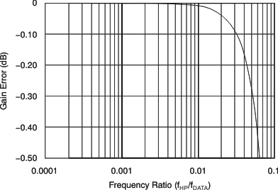
The HPF causes a small gain error, in which case the magnitude of the error depends on the ratio of ƒHP/ƒDATA. For many common values of (ƒHP/ƒDATA), the gain error is negligible. Figure 44 shows the gain error of the HPF. The gain error factor is illustrated in Equation 16 (see Device Support).
 Figure 44. HPF Gain Error
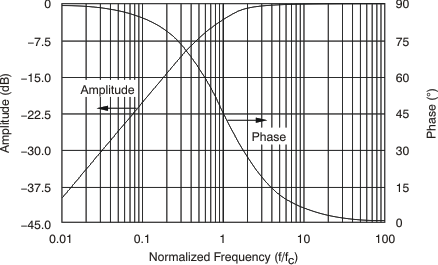
 Figure 45 shows the first-order amplitude and phase response of the HPF. In the case of applying step inputs or synchronizing, the settling time of the filter should be taken into account.
 Figure 45. HPF Amplitude and Phase Response