SBAS565C January   2014  â€“ August 2019 ADS1283

PRODUCTION DATA.  

  1. Features
  2. Applications
    1.     Simplified Schematic
  3. Description
  4. Revision History
  5. Pin Configuration and Functions
    1.     Pin Functions
  6. Specifications
    1. 6.1 Absolute Maximum Ratings
    2. 6.2 ESD Ratings
    3. 6.3 Recommended Operating Conditions
    4. 6.4 Thermal Information
    5. 6.5 Electrical Characteristics
    6. 6.6 Timing Requirements
    7. 6.7 Switching Characteristics
    8. 6.8 Typical Characteristics
  7. Parameter Measurement Information
    1. 7.1 Noise Performance
  8. Detailed Description
    1. 8.1 Overview
    2. 8.2 Functional Block Diagram
    3. 8.3 Feature Description
      1. 8.3.1 Analog Inputs and Multiplexer
      2. 8.3.2 Programmable Gain Amplifier (PGA)
      3. 8.3.3 Analog-to-Digital Converter (ADC)
        1. 8.3.3.1 Modulator
          1. 8.3.3.1.1 Modulator Overrange
          2. 8.3.3.1.2 Modulator Input Impedance
          3. 8.3.3.1.3 Modulator Overrange Detection (MFLAG)
          4. 8.3.3.1.4 Offset
          5. 8.3.3.1.5 Voltage Reference Inputs (VREFP, VREFN)
        2. 8.3.3.2 Digital Filter
          1. 8.3.3.2.1 Sinc Filter Stage (sinx / x)
          2. 8.3.3.2.2 FIR Stage
          3. 8.3.3.2.3 Group Delay and Step Response
            1. 8.3.3.2.3.1 Linear Phase Response
            2. 8.3.3.2.3.2 Minimum Phase Response
          4. 8.3.3.2.4 HPF Stage
      4. 8.3.4 Master Clock Input (CLK)
    4. 8.4 Device Functional Modes
      1. 8.4.1  Synchronization (SYNC PIN and SYNC Command)
        1. 8.4.1.1 Pulse-Sync Mode
        2. 8.4.1.2 Continuous-Sync Mode
      2. 8.4.2  Reset (RESET Pin and Reset Command)
      3. 8.4.3  Power-Down (PWDN Pin and STANDBY Command)
      4. 8.4.4  Power-On Sequence
      5. 8.4.5  DVDD Power Supply
      6. 8.4.6  Serial Interface
        1. 8.4.6.1 Chip Select (CS)
        2. 8.4.6.2 Serial Clock (SCLK)
        3. 8.4.6.3 Data Input (DIN)
        4. 8.4.6.4 Data Output (DOUT)
        5. 8.4.6.5 Serial Port Auto Timeout
        6. 8.4.6.6 Data Ready (DRDY)
      7. 8.4.7  Data Format
      8. 8.4.8  Reading Data
        1. 8.4.8.1 Read-Data-Continuous Mode
        2. 8.4.8.2 Read-Data-By-Command Mode
      9. 8.4.9  One-Shot Operation
      10. 8.4.10 Offset and Full-Scale Calibration Registers
        1. 8.4.10.1 OFC[2:0] Registers
        2. 8.4.10.2 FSC[2:0] Registers
      11. 8.4.11 Calibration Commands (OFSCAL and GANCAL)
        1. 8.4.11.1 OFSCAL Command
        2. 8.4.11.2 GANCAL Command
      12. 8.4.12 User Calibration
    5. 8.5 Programming
      1. 8.5.1 Commands
        1. 8.5.1.1  SDATAC Requirements
        2. 8.5.1.2  WAKEUP: Wake-Up From Standby Mode
        3. 8.5.1.3  STANDBY: Standby Mode
        4. 8.5.1.4  SYNC: Synchronize the Analog-to-Digital Conversion
        5. 8.5.1.5  RESET: Reset the Device
        6. 8.5.1.6  RDATAC: Read Data Continuous
        7. 8.5.1.7  SDATAC: Stop Read Data Continuous
        8. 8.5.1.8  RDATA: Read Data by Command
        9. 8.5.1.9  RREG: Read Register Data
        10. 8.5.1.10 WREG: Write to Register
        11. 8.5.1.11 OFSCAL: Offset Calibration
        12. 8.5.1.12 GANCAL: Gain Calibration
    6. 8.6 Register Maps
      1. 8.6.1 Register Descriptions
        1. 8.6.1.1 ID_CFG: ID_Configuration Register (address = 00h) [reset =x0h]
        2. 8.6.1.2 CONFIG0: Configuration Register 0 (address = 01h) [reset = 52h]
        3. 8.6.1.3 CONFIG1: Configuration Register 1 (address = 02h) [reset = 08h]
        4. 8.6.1.4 HPF0 and HPF1 Registers
          1. 8.6.1.4.1 HPF0: High-Pass Filter Corner Frequency, Low Byte (address = 03h) [reset = 32h]
          2. 8.6.1.4.2 HPF1: High-Pass Filter Corner Frequency, High Byte (address = 04h) [reset = 03h]
        5. 8.6.1.5 OFC0, OFC1, OFC2 Registers
          1. 8.6.1.5.1 OFC0: Offset Calibration, Low Byte (address = 05h) [reset = 00h]
          2. 8.6.1.5.2 OFC1: Offset Calibration, Mid Byte (address = 06h) [reset = 00h]
          3. 8.6.1.5.3 OFC2: Offset Calibration, High Byte (address = 07h) [reset = 00h]
        6. 8.6.1.6 FSC0, FSC1, FSC2 Registers
          1. 8.6.1.6.1 FSC0: Full-Scale Calibration, Low Byte (address = 08h) [reset = 00h]
          2. 8.6.1.6.2 FSC1: Full-Scale Calibration, Mid Byte (address = 09h) [reset = 00h]
          3. 8.6.1.6.3 FSC2: Full-Scale Calibration, High Byte (address = 0Ah) [reset = 40h]
  9. Application and Implementation
    1. 9.1 Application Information
    2. 9.2 Typical Applications
      1. 9.2.1 Geophone Interface
      2. 9.2.2 Digital Interface
    3. 9.3 Initialization Set Up
  10. 10Device and Documentation Support
    1. 10.1 Receiving Notification of Documentation Updates
    2. 10.2 Community Resources
    3. 10.3 Trademarks
    4. 10.4 Electrostatic Discharge Caution
    5. 10.5 Glossary
  11. 11Mechanical, Packaging, and Orderable Information

Package Options

Mechanical Data (Package|Pins)
Thermal pad, mechanical data (Package|Pins)
Orderable Information

Power-On Sequence

The ADS1283 has three power supplies: AVDD, AVSS, and DVDD. Figure 49 shows the power-on sequence of the ADS1283. The power supplies can be sequenced in any order. The supplies [the difference of (AVDD – AVSS) and DVDD] generate signals that are ANDed together for the internal reset. After the supplies have crossed the minimum thresholds, 216 fCLK cycles are counted before releasing the internal reset. After the internal reset is released, new conversion data are available, as shown in Figure 49 and Table 15.
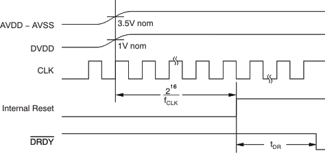
ADS1283 ai_tim_pwr_on_bas418.gifFigure 49. Power-On Sequence