SBAS559A May 2022 – December 2022 ADS1285
PRODUCTION DATA
- 1 Features
- 2 Applications
- 3 Description
- 4 Revision History
- 5 Pin Configuration and Functions
-
6 Specifications
- 6.1 Absolute Maximum Ratings
- 6.2 ESD Ratings
- 6.3 Recommended Operating Conditions
- 6.4 Thermal Information
- 6.5 Electrical Characteristics
- 6.6 Timing Requirements: 1.65 V ≤ IOVDD ≤ 1.95 V and 2.7 V ≤ IOVDD ≤ 3.6 V
- 6.7 Switching Characteristics: 1.65V ≤ IOVDD ≤ 1.95V and 2.7 V ≤ IOVDD ≤ 3.6 V
- 6.8 Timing Diagrams
- 6.9 Typical Characteristics
- 7 Parameter Measurement Information
-
8 Detailed Description
- 8.1 Overview
- 8.2 Functional Block Diagram
- 8.3 Feature Description
- 8.4 Device Functional Modes
- 8.5
Programming
- 8.5.1 Serial Interface
- 8.5.2 Conversion Data Format
- 8.5.3
Commands
- 8.5.3.1 Single Byte Command
- 8.5.3.2 WAKEUP: Wake Command
- 8.5.3.3 STANDBY: Software Power-Down Command
- 8.5.3.4 SYNC: Synchronize Command
- 8.5.3.5 RESET: Reset Command
- 8.5.3.6 Read Data Direct
- 8.5.3.7 RDATA: Read Conversion Data Command
- 8.5.3.8 RREG: Read Register Command
- 8.5.3.9 WREG: Write Register Command
- 8.5.3.10 OFSCAL: Offset Calibration Command
- 8.5.3.11 GANCAL: Gain Calibration Command
- 8.6
Register Map
- 8.6.1
Register Descriptions
- 8.6.1.1 ID/SYNC: Device ID, SYNC Register (Address = 00h) [Reset = xxxx0000b]
- 8.6.1.2 CONFIG0: Configuration Register 0 (Address = 01h) [Reset = 12h]
- 8.6.1.3 CONFIG1: Configuration Register 1 (Address = 02h) [Reset = 00h]
- 8.6.1.4 HPF0, HPF1: High-Pass Filter Registers (Address = 03h, 04h) [Reset = 32h, 03h]
- 8.6.1.5 OFFSET0, OFFSET1, OFFSET2: Offset Calibration Registers (Address = 05h, 06h, 07h) [Reset = 00h, 00h, 00h]
- 8.6.1.6 GAIN0, GAIN1, GAIN2: Gain Calibration Registers (Address = 08h, 09h, 0Ah) [Reset = 00h, 00h, 40h]
- 8.6.1.7 GPIO: Digital Input/Output Register (Address = 0Bh) [Reset = 000xx000b]
- 8.6.1.8 SRC0, SRC1: Sample Rate Converter Registers (Address = 0Ch, 0Dh) [Reset = 00h, 80h]
- 8.6.1
Register Descriptions
- 9 Application and Implementation
- 10Device and Documentation Support
- 11Mechanical, Packaging, and Orderable Information
Package Options
Mechanical Data (Package|Pins)
- RHB|32
Thermal pad, mechanical data (Package|Pins)
- RHB|32
Orderable Information
8.3.6.2 FIR Filter Section
The second section of the digital filter is a multistage, FIR low-pass filter. Partially filtered data from the sinc filter are input to the FIR filter. The FIR filter determines the final frequency and phase response of the data. Figure 8-14 shows that the FIR filter consists of four stages.
The first two FIR stages are half-band filters with decimation = 2 for each stage. The third and fourth FIR stages determine the final frequency and phase response. Decimation is 4 and 2, for FIR stages three and four. The overall decimation ratio of the FIR filter is 32. Unique coefficient sets in stage 3 and 4 determine linear and minimum phase filter response. The phase response is selected by the PHASE bit of the CONFIG0 register. Table 8-4 lists the combined decimation ratio of the sinc and FIR filter stages and the corresponding FIR filter data rate.
| DR[2:0] BITS | COMBINED DECIMATION RATIO | DATA RATE (SPS) | |
|---|---|---|---|
| HIGH- AND MID-POWER MODES | LOW-POWER MODE | ||
| 000 | 8192 | 250 | 125 |
| 001 | 4096 | 500 | 250 |
| 010 | 2048 | 1000 | 500 |
| 011 | 1024 | 2000 | 1000 |
| 100 | 512 | 4000 | 2000 |
Table 8-5 lists the FIR filter coefficients and the data scaling for the linear and minimum phase coefficients.
| COEFFICIENT | STAGE 1 | STAGE 2 | STAGE 3 | STAGE 4 | ||
|---|---|---|---|---|---|---|
| SCALE = 1/512 | SCALE = 1/8388608 | SCALE = 1/134217728 | SCALE = 1/134217728 | |||
| LINEAR PHASE | LINEAR PHASE | LINEAR PHASE | MINIMUM PHASE | LINEAR PHASE | MINIMUM PHASE | |
| b0 | 3 | –10944 | 0 | 819 | –132 | 11767 |
| b1 | 0 | 0 | 0 | 8211 | –432 | 133882 |
| b2 | –25 | 103807 | –73 | 44880 | –75 | 769961 |
| b3 | 0 | 0 | –874 | 174712 | 2481 | 2940447 |
| b4 | 150 | –507903 | –4648 | 536821 | 6692 | 8262605 |
| b5 | 256 | 0 | –16147 | 1372637 | 7419 | 17902757 |
| b6 | 150 | 2512192 | –41280 | 3012996 | –266 | 30428735 |
| b7 | 0 | 4194304 | –80934 | 5788605 | –10663 | 40215494 |
| b8 | –25 | 2512192 | –120064 | 9852286 | –8280 | 39260213 |
| b9 | 0 | 0 | –118690 | 14957445 | 10620 | 23325925 |
| b10 | 3 | –507903 | –18203 | 20301435 | 22008 | –1757787 |
| b11 | 0 | 224751 | 24569234 | 348 | –21028126 | |
| b12 | 103807 | 580196 | 26260385 | –34123 | –21293602 | |
| b13 | 0 | 893263 | 24247577 | –25549 | –3886901 | |
| b14 | –10944 | 891396 | 18356231 | 33460 | 14396783 | |
| b15 | 293598 | 9668991 | 61387 | 16314388 | ||
| b16 | –987253 | 327749 | –7546 | 1518875 | ||
| b17 | –2635779 | –7171917 | –94192 | –12979500 | ||
| b18 | –3860322 | –10926627 | –50629 | –11506007 | ||
| b19 | –3572512 | –10379094 | 101135 | 2769794 | ||
| b20 | –822573 | –6505618 | 134826 | 12195551 | ||
| b21 | 4669054 | –1333678 | –56626 | 6103823 | ||
| b22 | 12153698 | 2972773 | –220104 | –6709466 | ||
| b23 | 19911100 | 5006366 | –56082 | –9882714 | ||
| b24 | 25779390 | 4566808 | 263758 | –353347 | ||
| b25 | 27966862 | 2505652 | 231231 | 8629331 | ||
| b26 | 25779390 | 126331 | –215231 | 5597927 | ||
| b27 | 19911100 | –1496514 | –430178 | –4389168 | ||
| b28 | 12153698 | –1933830 | 34715 | –7594158 | ||
| b29 | 4669054 | –1410695 | 580424 | –428064 | ||
| b30 | –822573 | –502731 | 283878 | 6566217 | ||
| b31 | –3572512 | 245330 | –588382 | 4024593 | ||
| b32 | –3860322 | 565174 | –693209 | –3679749 | ||
| b33 | –2635779 | 492084 | 366118 | –5572954 | ||
| b34 | –987253 | 231656 | 1084786 | 332589 | ||
| b35 | 293598 | –9196 | 132893 | 5136333 | ||
| b36 | 891396 | –125456 | –1300087 | 2351253 | ||
| b37 | 893263 | –122207 | –878642 | –3357202 | ||
| b38 | 580196 | –61813 | 1162189 | –3767666 | ||
| b39 | 224751 | –4445 | 1741565 | 1087392 | ||
| b40 | –18203 | 22484 | –522533 | 3847821 | ||
| b41 | –118690 | 22245 | –2490395 | 919792 | ||
| b42 | –120064 | 10775 | –688945 | –2918303 | ||
| b43 | –80934 | 940 | 2811738 | –2193542 | ||
| b44 | –41280 | –2953 | 2425494 | 1493873 | ||
| b45 | –16147 | –2599 | –2338095 | 2595051 | ||
| b46 | –4648 | –1052 | –4511116 | –79991 | ||
| b47 | –874 | –43 | 641555 | –2260106 | ||
| b48 | –73 | 214 | 6661730 | –963855 | ||
| b49 | 0 | 132 | 2950811 | 1482337 | ||
| b50 | 0 | 33 | –8538057 | 1480417 | ||
| b51 | 0 | 0 | –10537298 | –586408 | ||
| b52 | 9818477 | –1497356 | ||||
| b53 | 41426374 | –168417 | ||||
| b54 | 56835776 | 1166800 | ||||
| b55 | 41426374 | 644405 | ||||
| b56 | 9818477 | –675082 | ||||
| b57 | –10537298 | –806095 | ||||
| b58 | –8538057 | 211391 | ||||
| b59 | 2950811 | 740896 | ||||
| b60 | 6661730 | 141976 | ||||
| b61 | 641555 | –527673 | ||||
| b62 | –4511116 | –327618 | ||||
| b63 | –2338095 | 278227 | ||||
| b64 | 2425494 | 363809 | ||||
| b65 | 2811738 | –70646 | ||||
| b66 | –688945 | –304819 | ||||
| b67 | –2490395 | –63159 | ||||
| b68 | –522533 | 205798 | ||||
| b69 | 1741565 | 124363 | ||||
| b70 | 1162189 | –107173 | ||||
| b71 | –878642 | –131357 | ||||
| b72 | –1300087 | 31104 | ||||
| b73 | 132893 | 107182 | ||||
| b74 | 1084786 | 15644 | ||||
| b75 | 366118 | –71728 | ||||
| b76 | –693209 | –36319 | ||||
| b77 | –588382 | 38331 | ||||
| b78 | 283878 | 38783 | ||||
| b79 | 580424 | –13557 | ||||
| b80 | 34715 | –31453 | ||||
| b81 | –430178 | –1230 | ||||
| b82 | –215231 | 20983 | ||||
| b83 | 231231 | 7729 | ||||
| b84 | 263758 | –11463 | ||||
| b85 | –56082 | –8791 | ||||
| b86 | –220104 | 4659 | ||||
| b87 | –56626 | 7126 | ||||
| b88 | 134826 | –732 | ||||
| b89 | 101135 | –4687 | ||||
| b90 | –50629 | –976 | ||||
| b91 | –94192 | 2551 | ||||
| b92 | –7546 | 1339 | ||||
| b93 | 61387 | –1103 | ||||
| b94 | 33460 | –1085 | ||||
| b95 | –25549 | 314 | ||||
| b96 | –34123 | 681 | ||||
| b97 | 348 | 16 | ||||
| b98 | 22008 | –349 | ||||
| b99 | 10620 | –96 | ||||
| b100 | –8280 | 144 | ||||
| b101 | –10663 | 78 | ||||
| b102 | –266 | –46 | ||||
| b103 | 7419 | –42 | ||||
| b104 | 6692 | 9 | ||||
| b105 | 2481 | 16 | ||||
| b106 | –75 | 0 | ||||
| b107 | –432 | –4 | ||||
| b108 | –132 | 0 | ||||
| b109 | 0 | 0 | ||||
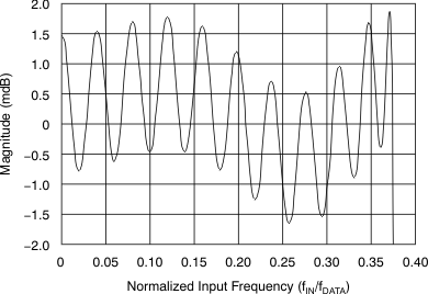
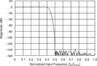
Figure 8-15 shows the FIR pass-band frequency response to 0.375 × fDATA with ±0.003-dB pass-band ripple. Figure 8-16 shows the pass-band, transition-band, and stop-band performance from 0 Hz to fDATA. The filter is designed for –135-dB stop-band attenuation at the Nyquist frequency.
 Figure 8-15 FIR Filter
Pass-Band Response
 Figure 8-16 FIR Filter
Transition Band Response
Figure 8-16 FIR Filter
Transition Band ResponseAs with many sampled systems, the filter response repeats at multiples of the modulator sample rate (fMOD). The filter response repeats at frequencies = N × fMOD ± f0, where N = 1, 2, and so on, and f0 = filter pass-band). These frequencies, if not filtered and are otherwise present in the signal, fold back (or alias) into the pass-band causing errors. A low-pass input filter reduces the aliasing error. For a band-limited signal typical of many geophones, a single-pole filter at the PGA output is sufficient to suppress the aliasing frequencies.